Keywords
|
| Inverter, Microcontroller, MOSFET,PWM. |
I.INTRODUCTION
|
| The current trend of increasing paradigm shift in power generation and distribution towards renewable and alternative energy sources have given rise to excessive importance to distributed energy systems. Since the power harnessing and storage from most of these sources are as DC, it needs to be converted to AC for compatibility with the existing AC power systems. Inverter converts regulated DC voltage to AC voltage [1].Developing an optimized renewable energy harnessing system is a very lucrative area in the power industry. |
| This paper describes a method to design a single phase sine wave inverter using IGBT as switching devices to obtain a sine wave AC output of desired magnitude and frequency, and analyze the effect of various passive components on the output waveform and try to improve the quality of the waveform. The desired output waveform should be a sine-wave with very low harmonic distortion and clean power like utility supplied electricity. The pure sine wave inverters have the advantages such as: Inductive loads like microwaves and motors run faster, quieter and cooler. It reduces audible and electrical noise in fans, fluorescent lights, audio amplifiers, TV, fax and answering machines. It Prevents crashes in computers and glitches in monitors [2]. |
| Any device that uses a control circuitry that senses the phase (for voltage / speed control) or instantaneous zero voltage crossing (for timing control) will not work properly from a voltage that has a modified sine wave-form. Also, as the modified sine wave is a form of square wave, it is comprised of multiple sine waves of odd harmonics (multiples) of the fundamental frequency of the modified sine wave. For example, a 60 Hz. modified sine wave will consist of sine waves with odd harmonic frequencies of 3rd (180 Hz), 5th (300 Hz.), and 7th (420 Hz.) and so on[3]. The high frequency harmonic content in a modified sine wave produces enhanced radio interference, higher heating effect in motors / microwaves and produces overloading due to lowering of the impedance of low frequency filter capacitors / power factor improvement capacitors. |
II. LITERATURE SURVEY
|
| The developments in power electronics and semiconductor technology have triggered the improvements in power electronic systems. The main components of a driving circuit for an inverter consist of power circuit, driver circuit, user interface, mathematical models and serial transmission of data to the microcontroller. Based on power supply inverters can be classified into two types : voltage source inverter and current source inverter. A VSI has small or negligible impedance at it’s input terminal that is, it has a stiff DC voltage source, where as for a CSI, it is fed with adjustable current from a DC source with high impedance. |
| Recently, microcontrollers and digital signal processors (DSP) are used as advanced control techniques. Many researchers developed the software for the control system, which confirmed the high quality of the control based on microcontroller techniques [4] and to provide additional real time processing throughput in an inverter operation, |
| microcontrollers and DSP features minimize the CPU's overhead in an interrupt intensive application [5]. |
III.WORKING OF A SINGLE PHASE INVERTER
|
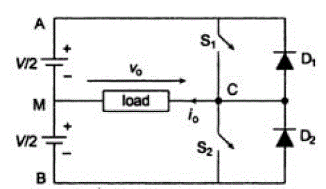
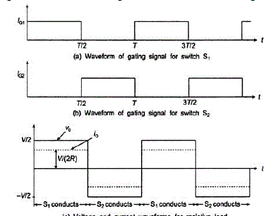
| The Fig. 1 shows the gating signals IG1 and IG2 of switches S1 and S2 respectively. The switch S1 is closed for half time period (T/2) of the desired ac output. It connects point A of the dc source to point C and the output voltage Vo becomes equal to +V/2. |
| At t=T/2, gating signal is removed from S1 and it turns off. For the next half time period (T/2<t<T), the gating signal is given to S2. It connects point B of the dc source to point C and the output voltage reverses. Thus, by closing S1 and S2 alternately, for half time periods, a square-wave ac voltage is obtained at the output. |
| For a resistive load, the load current is given by: |
| Io=Vo/R |
| Hence, the wave shape of output current is identical to that of output voltage, as show in Fig. 2 |
| The frequency of output voltage is given by: |
| f=1/t |
| By controlling the time periods of the gate-drive signals, the frequency can be varied. |
IV.METHODOLOGY
|
3.1 CONTROL CIRCUIT
|
| The control circuit generates complementary pulses for IGBT switching on and switching off. Complementary pulses are needed for triggering the IGBTs. These are square wave pulses of magnitude 5V (approx.). In order to ensure proper commutation of the IGBTs, a blanking time of approximately 100μSec (for an IGBT) has been introduced [6]. This is to make sure that both the IGBT are not switched on simultaneously (short-circuited). |
A.SOFTWARE IMPLEMENTATION
|
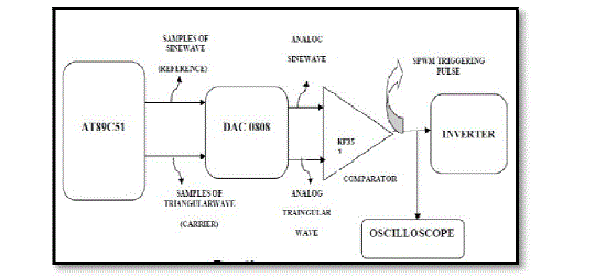
| The Block diagram representation of wave generation scheme is shown in Fig. 3. The AT89C51 microcontroller is used to generate PWM pulses [7] to trigger the Power Circuit. The Generation of Digital Sample of Sinusoidal and Triangular waves from the microcontroller are fed into the DAC 0808 and the analog output from the DAC 0808 is fed into the comparator KF351 which compares the analog output from the DAC. The comparator gives SPWM triggering pulses which is observed through the Oscilloscope and fed to the inverter. |
| The 8051 C Language programming for wave generation is used here to generate triangular and sine wave output from the microcontroller. |
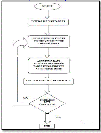
| The flowchart representation for microcontroller wave generation is shown in Fig. 4.The Sine and the triangular waves generated are converted to analog signals using a digital to analog converter (Dual DAC) and the output is given to Op- Amp (μA741). |
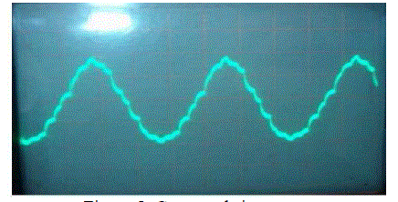
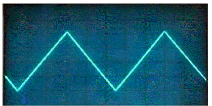
| The Output of the Dual DAC is viewed using the CRO and the output is as shown in Fig. 5 and Fig. 6. |
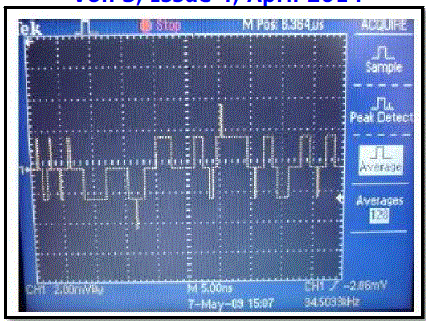
| The sine wave output terminal from the Dual DAC is connected to the 470K potentiometer which acts as a voltage divider circuit and amplitude of the sine wave can be varied accordingly. Now the outputs are given to the Op-Amp and the PWM signal is obtained as shown in Fig. 7. The PWM signal [8] is the output signal of control circuit which is given as input to the gates of IGBTs of power circuit. |
3.2 POWER CIRCUIT
|
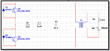
| The Power circuit is a push-pull inverter circuit having two IGBTs acting as switches connected to transformer primary winding with resistance and inductance in series. Load is connected to secondary winding of the transformer as shown in Fig. 8. Control voltage is applied between gate and emitter of IGBT and DC supply voltage which is to be converted to ac voltage is applied across collector and emitter of IGBT. The power circuit is as shown in the Fig. 8. |
| The current flows through IGBT and the corresponding circuit including half the number of primary winding of the transformer when IGBT is turned on. Complemented pulses are given to the IGBTs so that they turn on alternatively and cause a Current flow through the upper and lower half of the primary winding alternatively and in opposite direction. Resultant output which is taken across the load connected to secondary winding will be alternating sine wave. |
| Resistance and inductance are used in series with switches to limit the sudden change in current (di/dt effect). Transformer is used to provide isolation and flexibility in the circuit i.e. transformer ratio is chosen according to the required output voltage. |
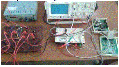
| The complete hardware experimental setup is shown in Fig. 9. |
V.RESULT AND OUTPUT ANALYSIS
|
| The output waveform obtained at the load connected to secondary of the transformer is distorted sine wave. We analyze the effect of various components in the circuit on the output waveform and try to improve the wave form using capacitance, inductance and diodes across the load. |
1. EFFECT ON RESISTIVE LOAD (WITH AND WITHOUT DIODE)
|
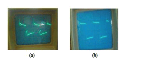
| Anti-parallel diodes were connected across switches to prevent the large power dissipation in switches when inductive loads are connected to the circuit by reducing the current stress on IGBT and aiding the commutation. Theoretically there is no need of anti-parallel diodes across switches for R load. Since we are using a large transformer some inductance was added in the circuit and hence even with the R load we are able to observe considerable reduction in over shoot and significant improvement in the waveform by connecting anti parallel diodes to the IGBT’s. The output waveform on the CRO can be seen in Fig. 10. |
| Initially the waveform had large overshoot as can be seen in Fig. 10(a) but after the diodes have been connected across the load the overshoot has been reduced greatly which can be observed in Fig. 10(b) |
2. EFFECT OF CAPACITIVE LOAD
|
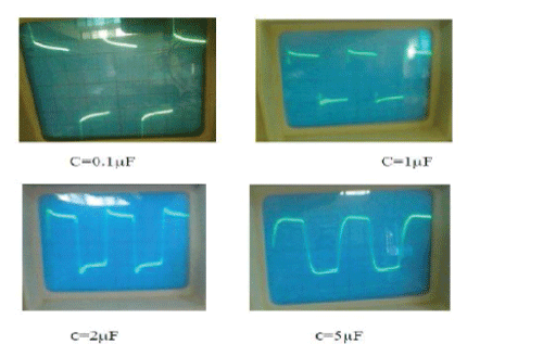
| As we have large overshoots in the wave form a capacitance is used across R load to control the overshoot. The value of capacitance added with a fixed resistance value of R=750Ω and its effect on the output waveform is as shown in Fig.11. As the value of capacitance included across the load increases the overshoot reduces. The overshoot is minimal with capacitance of 5uF.It can be observed that by connecting a capacitance of 5uF across the load the waveform has improved considerably as compared to the waveform when capacitance of 0.1uF was connected across the load. |
3. EFFECT OF INDUCTIVE LOAD
|
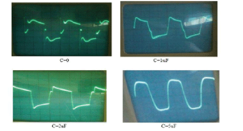
| Inductive load test is one of the desirable tests for the circuit and for the stability of wave form. An inductance of 5H is connected in series with the 750Ω resistance and wave forms are observed by changing the capacitance values across the load as shown in Fig. 12. |
| With inductive load wave forms tend to be more distorted at normal operation. It can be corrected by connecting a large capacitance in parallel with the load. It can be observed that as the value of capacitance connected is increased from 0uF to 5uF the distortion reduces and with capacitance of 5uF the waveform obtained across the load is almost a sinusoidal waveform. |
VI.CONCLUSION
|
| The single phase inverter was realized using two IGBTs in parallel inverter configuration and the output waveforms across the resistive load of 1K in the power circuit were obtained and were found to be sine waves. The output was studied for resistive and inductive load and was found to be sine wave with minimal overshoot, hence satisfactory. |
| The different parts of the Inverter: the control circuit, the gating circuit and the power circuit or inverter circuit were successfully linked to each other and the outputs of each stage were obtained. By analyzing various waveforms and the effect of various components on the waveform we can say that voltage and current stress on the switches lead to wave form distortion. By reducing the voltage and current stresses on the switches and ensuring proper commutation, waveform can be improved. |
| The output sine wave can be further improved by incorporating harmonic filters at both input and output ends. |
| |
Figures at a glance
|
 |
 |
 |
 |
| Figure 1 |
Figure 2 |
Figure 3 |
Figure 4 |
 |
 |
 |
 |
| Figure 5 |
Figure 6 |
Figure 7 |
Figure 8 |
 |
 |
 |
 |
| Figure 9 |
Figure 10 |
Figure 11 |
Figure 12 |
|
| |
References
|
- Maria D. Bellar, Tzong-Shiann Wu, Aristide Tchamdjau, JavadMahdavi and M.Ehsani, “A Review of Soft-switched DC-AC Converter”, IEEEtransactions On Industry Applications, vol. 43, no. 4, pp. 847-858,1998.
- Muhammad H. Rashid, 2004, “Power Electronics: Circuit’s Devices and Applications”, Prentice Hall: 226-299.
- Ashfaq Ahmed, 1999, “Power Electronic and Technology”, Prentice Hall: 304-327.
- L. Rimifriu, M. Lucanu, C, Aghion, O. Ursaru, “Control With Microcontroller For PWM Single-Phase Inverter,” IEEE, "Gh. Asachi" TechnicalUniversity of Iasi, Faculty of Electronics and Telecommunications, Bd. Carol I, no. 11, Iasi, 700537 Romania. 2003.
- W. Bacharowski, “Microcontrollers in Variable Frequency Inverters”, WESCON95, Maintain View, CA, Conference Record, MicroelectronicsCommunications Technology Producing Quality Products Mobile and Portable Power Emerging Technologies, 1995, pp. 13-15.
- A.C. Oliveira, A.M.N. Lima and C.B. Jacobina, “Varying the Switching Frequency to Compensate the Dead-time in Pulse Width ModulatedVoltage Source Inverter”, power electronics specialist conference, 2002.pese 02.2002.IEEE 33rd annual conference vol I, pp. 244- 249,2002
- R. Wu. S. B. Dewan, and G. R. Slemon, “A PWM ac to dc converter with fixed switching frequency,” in Rec. /EEE /AS Annual Meeting, pp.706-711, 1988.
- A. Tahri, A. Draou and M.Ermis,”A Comparative Study of PWM Control Techniques for Multilevel Cascaded Inverters”, Applied PowerElectronics Laboratory, Department of Electrotechnics, University of Sciences and Technology of Oran,Algeria.
|