Keywords
|
| DVR, Voltage sag, Voltage swell, Harmonics and Matrix converter |
INTRODUCTION
|
| One of the major concerns in electricity industry today is power quality problems to sensitive loads. This is due to the advent of a large numbers of sophisticated electrical and electronic equipment, such as computers, programmable logic controllers and variable speed drives etc. The use of these equipments very often requires power supplies with very high quality. Voltage sag, which is a momentary decrease in rms voltage magnitude in the range of 0.1 to 0.9 per unit (p.u.), is considered as the most serious problem of power quality. It is often caused by faults in power systems or by starting of large induction motors. It can interrupt or lead to malfunction of any electric equipment which is sensitive to voltage variations. It occurs more frequently than any other power quality phenomenon does. Therefore, the loss resulted due to voltage sag problem for a customer at the load-end is huge. Voltage swell is defined as an increase in RMS voltage from 1.1 to 1.8 per unit in power frequency and during half cycle to 1 minute. Like the voltage sag, voltage swell is related to faults in power system, but is not that common. Unloading large inductive loads and energizing large capacitor banks are the possible reasons of the voltage swell [1]. |
| The use of a Dynamic Voltage Restorer (DVR) known as voltage sag compensator, is one of the most effective solutions to restoring the quality of voltage at its load-side terminals when the quality of voltage at its source-side terminals is disturbed. DVR is superior to the uninterruptible power supply (UPS) in cost and efficiency, because the DVR has a smaller converter rating than the UPS. In terms of minimum apparent power injection or size of the coupling transformer, the performance of a DVR is found to be superior to a Distribution Static Synchronous Compensator (DSTATCOM) [2]. Traditional DVR topologies are categorized into two groups. The first group uses AC/DC/AC conversion [3]. In this topology, the required dc voltage is provided through a transformer from the grid (source side or load side) via a rectifier, a dc link capacitor and inverter. In the second group, the required energy for compensation of voltage is taken from the external dc capacitor or another energy storage element such as a doublelayer capacitor, superconducting magnet or lead-acid battery via an inverter [4]. These types of topologies cannot compensate voltage sag and swell for a long time due to the limitation of stored energy. In both topologies, it is necessary to embed a large capacitor in the dc link. The cost of this dc-link capacitor is high and it results in high cost. |
| However, the need for reduction in cost, weight and physical size has inhibited the DVR from greater penetration and wider acceptance [5], [6]. |
| In this paper, a new topology is used for DVR which does not have dc link. A converter with the ability of AC-AC conversion with no dc link is required to eliminate the energy storing elements. The converter with this characteristic is called matrix converter (MC) [7] which uses a matrix of semiconductor or bi-directional switches. There are many control methods used to generate PWM signals for matrix converters such as venturini method, sinusoidal PWM method, sampled PWM method and hysteresis control method etc. Among these control methods Least Mean Square Error (LMSE) method is most efficient because this method is able to produce undistorted and balanced output voltages, even if the input supply voltages are distorted and unbalanced. In this method, the switches working with low frequency, therefore by this method the matrix converter has minimum switching loss. As a result, the efficiency of the converter will be high and THD is very less when compared to other methods. Here a three-phase to single-phase matrix converter is considered and Least Mean Square Error method is used. In this method, we compare the real output with the reference output, and the errors generated identify the switches that must be ON, and the switches that must be OFF. |
| In this paper, the power circuit of the new DVR is initially contemplated and its control method is described then. The simulation results in PSCAD software admit the ability of proposed structure in compensating balanced and unbalanced voltage sag, voltage swell and extreme voltage disturbances. |
II. STRUCTURE OF DVR WITH MATRIX CONVERTER
|
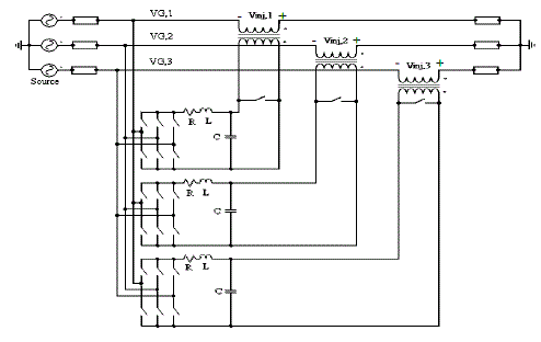
| The power circuit for the proposed DVR is shown in Fig. 1. In this structure, 3 three-phase to single-phase MCs are used to eliminate dc link. The MCs are directly connected to the source and their produced voltage is again injected to the grid through three single-phase transformers [8]. These transformers prevent the phases to be short-circuited, because MCs connect the input voltages to output directly. Considering Fig. 1, the voltage equations of load would be given in eq. 1 as follows: |
 |
| In eq (1), L, G and inj subscripts are used to represent load, source and DVR respectively. Also, a, b, c subscripts are used to show the first, second and third phases. |
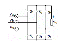
| When the source produces the rated voltage, the MC does not produce any voltage. So the load voltage will be same as that of source voltage. When any voltage sag or swell occur at source side, the MC produces the necessary voltage according to that voltage sag or swell, and injects it to the grid through transformers. The injecting voltage will be in same polarity with source voltage in voltage sag condition and in opposite polarity with source voltage in the voltage swell condition. Therefore, a voltage with fixed amplitude is produced on load side. Unbalanced voltage sag and swell can be compensated through independent MCs. If one of the DVR’s phases encounters power quality problem, other phases will continue to operate correctly. Three-phase to single-phase MCs, can be developed using 6 bi-directional switches and so they can block voltage with any polarity and they can conduct the current in both directions. There are several arrangements to create a bi-directional switch. In this paper, the common emitter topology has been used. A MC with 6 bi-directional power switches is shown in Fig. 2 [9]. This converter can produce 64 different switching modes. These switching modes are reduced to 7 modes by considering the following two facts given below, |
| ïÃâ÷ Avoid short circuit on input side |
| ïÃâ÷ Avoid open circuit on load side |
| The seven switching modes or voltage levels obtained from this converter is given in Table I. |
III. CONTROL STRATEGY
|
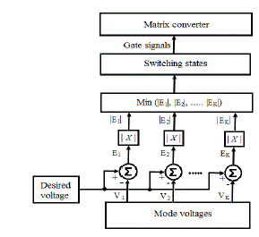
| The control strategy used to control MCs is LMSE method [10]. This control method is based on the minimum error between the desired output voltage and the produced voltage. Fig. 3 shows the block diagram of the control circuit of the matrix converters used in DVR structure. In this strategy, the error exists between the desired output voltage and produced voltage for different operating modes of matrix converters are given in eq. 2 as follows: |
 |
| Where Ei(t) is the error obtained at ith mode, Vo, Desired and Vo,Mode,i is the desired voltage and mode voltage respectively. |
| In this control method, the output voltage in different modes is compared with the desired output, and the error is calculated for each operating mode. After calculating the absolute values of these errors, the minimum error is recognized using “minimum” block. The switching states in different modes are saved in the look-up table. So according to the mode chosen by “minimum” block, turn on and turn off signals for the switches are chosen from the look-up table and are sent to matrix converter through driver circuits [11]. The look up table function is as follows: |
 |
| This control strategy results in reduction of switching numbers and consequently considerable reduction in converter losses and increase in its efficiency. By this strategy dv/dt stresses over power switches in MCs are significantly reduced. Also, it is possible to operate with low speed semiconductors. |
IV. SIMULATION RESULTS
|
| The performance of DVR with matrix converter using LMSE method was evaluated by computer simulation using PSCAD/EMTDC toolbox. The DVR is connected between the PCC and sensitive load by means of a 2 kVA transformer with 0.25 turns ratio and a star connected secondary. The system was tested under the following conditions shown in Table II. |
| In the test system, the matrix converter is connected at source side of the system. The active power required for the compensation should be taken from the supply side. So it can compensate long time sag and swell and there is no need of energy storage elements. Simulation results show for the case of both balanced and unbalanced fault such as voltage sag and swell and for the case of distorted input. |
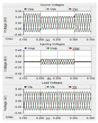
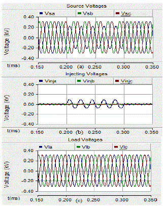
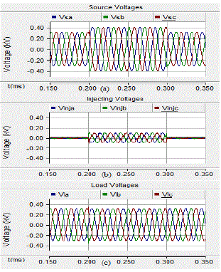
| The simulation results shown in fig. 4 and fig. 5 represent balanced and unbalanced voltage sag respectively. In the test system, during t = 0.2s to 0.3s, a voltage sag is applied in all the three phases. Then the source voltage is reduced to 155V from 220V. DVR injects 59V to compensate the load voltage. In the case of unbalanced sag, a single phase fault is applied at phase ‘a’ during 0.2s to 0.3s. To compensate the load voltage DVR injects 64V. |
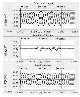
| In the case of balanced voltage swell, swell is applied in three phases at t = 0.2s and the duration is 0.1s. At this time, the input voltage is increased to 283V from 220V. The DVR injects 68V in opposite phase through the series transformer to the faulted line for compensation. In the case of unbalanced swell, the voltage in phase ‘a’, then voltage is increased up to 283V at t= 0.2s to 0.3s. DVR injects 74V in opposite phase. The simulation results are shown in Fig.6 and Fig.7 respectively. |
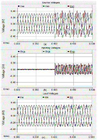
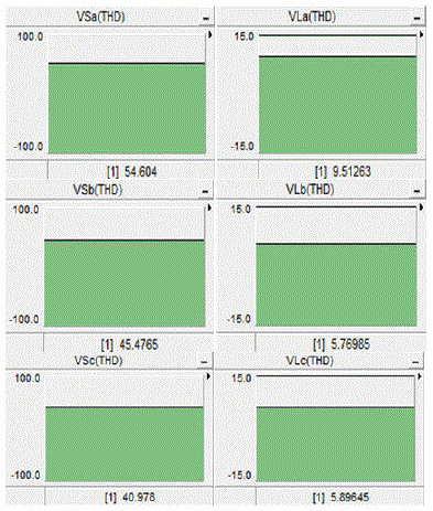
| waveform’s fundamental frequency. In this case, the test system is provided with harmonics for a period 0.4s to 0.5s. During this period DVR provides better voltage with less disturbances at load. Simulation results and THD analysis are shown in Fig.8 and Fig.9 respectively. In this time interval the source voltage is extremely distorted as presented in eq (3). In each of these abnormal conditions, the DVR comes into play and injects required voltage to the grid. So the new structure can compensate several voltage disturbances such as balanced and unbalanced voltage sag, swell and harmonics. |
 |
V. CONCLUSION
|
| In this paper a new topology called matrix converter is applied for DVRs to eliminate dc link. There by the system cost will be reduced. Three independent three-phase to single-phase MCs are used to inject compensating voltage to the line via transformer. As a result, this DVR structure can be used to restore load voltage in both balanced and unbalanced voltage sag and swell conditions. Also, one of the main advantages of the proposed DVR is voltage restoration capability in an extremely disturbed network. From the simulation results it is clear that this DVR topology is able to compensate several power quality problems such as voltage sag and swell both balanced and unbalanced cases successfully and the THD is very less. It provides fast response and has high efficiency. |
Tables at a glance
|
 |
 |
| Table 1 |
Table 2 |
|
Figures at a glance
|
 |
 |
 |
 |
 |
| Figure 1 |
Figure 2 |
Figure 3 |
Figure 4 |
Figure 5 |
 |
 |
 |
 |
| Figure 6 |
Figure 7 |
Figure 8 |
Figure 9 |
|
| |
References
|
- Scott D. MacGregor, “An Overview of Power Quality Issues and Solutions”, IEEE Cement Industry Conference, Rapid City, South Dakota,May 17 - 21, 1998.
- Stump, M.D. Keane and G.J., and Leong, “The Role of Custom Power Products in Enhancing Power Quality at Industrial Facilities”, IEEEEnergy Management and Power Del., vol.6 no.2, pp. 507-517, July 1998.
- J. G. Nielsen and F. Blaabjerg, “A Detailed Comparison of System Topologies for Dynamic Voltage Restorers”, IEEE Trans. Ind. App., vol. 41,no.5, pp. 272-1280, Sep. /Oct. 2005.
- V. K. Ramachandaramurthy, C. Fitzer, A. Arulampalam, C. Zhan, M. Barnes, and N. Jenkins, “Control of a battery supported dynamic voltagerestorer,” Proc. IEE, Gen., Transm. and Dist., vol. 149, pp. 533-542, 2002.
- M. H. Haque, “Compensation of Distribution System Voltage Sag by DVR and DSTATCOM”, IEEE Porto Power Technical Conference, vol.1, June 2002.
- T. Jimichi, H. Fujita, and H. Akagi, “Design and Experimentation of a Dynamic Voltage Restorer Capable of Signi_cantly Reducing an EnergyStorage Element”, IEEE Trans. Ind. App., vol. 44, no.3, pp. 817-825, May/June 2008.
- Patrick W. Wheeler, Jose Rodriguez, Jon C. Clare, Lee Empringham, and Alejandro Weinstein, “Matrix Converters: A Technology Review”,IEEE Trans. Ind. Electron., vol. 49, no.2, pp. 276-288, April 2002.
- E. Babaei, M. FarhadiKangarlu and M. Sabahi, “Mitigation of Voltage Disturbances Using Dynamic Voltage Restorer based on DirectConverters”, IEEE Trans. Power Del., vol. 25, no.4, pp. 2676-2683, Oct. 2010.
- Khanmohammadi, “A New Structure for Three-Phase to Single-Phase AC/AC Matrix Converters,” 10th IEEE International Conference onElectronics, Circuits and Systems (ICECS2003), University of Sharjah, United Arab Emirates, vol. I, pp. 36-39, 2003.
- Khanmohammadi S.; Aghagolzadeh A.; Hosseini S. H, E.Babaei, “A New Algorithm for Three-Phase to Single-Phase AC/AC MatrixConverters”, Proc. ICECS, vol. 3, pp. 1121-1124, Dec. 2003.
- E. Babaei, Ali AghabeigiHeris, “PWM-Based Control Strategy for Forced Commutated Cycloconverters”, IEEE Symposium on Ind. Electron.and App. (ISIEA 2009), Kuala Lumpur, Malaysia, pp. 669-674, 2009.
- E. Babaei and M. F. Kangarlu, “A New Topology for Dynamic Voltage Restorers without DC Link”, Proc. ISIEA, Malaysia, pp. 1009-1014, Oct. 2009.
|