Keywords
|
| Cascaded H-bridge multilevel inverter (CHB), phase shifted modulation, multicarrier pulse-width modulation, total harmonic distortion (THD). |
INTRODUCTION
|
| Over the past two decades, multilevel inverters have attracted wide interest both in the scientific community and in the industry. The reason for the increased interest is that the multilevel inverters are a viable technology to implement controlled rotational movement in high-power applications. Multilevel inverters include an array of power semiconductors and capacitor voltage sources, the output of which generate voltages with stepped waveforms. The commutation of the switches permits the addition of the capacitor voltages, which reach high voltage at the output, while the power semiconductors must withstand only reduced voltages. Multilevel converters have a lot of advantages to offer in medium- to high-voltage range of applications. These include variable speed motor drives and power system applications. Multilevel converters can synthesize waveforms using more than two voltage levels, Small filter components are required and sometimes they can be left out altogether. Disadvantages of multilevel topologies include: high number of semiconductor devices, complex control as a result of the large number of controlled devices, large number of gate drive circuits, several DC voltage sources are required, need to balance voltages across capacitors used in voltage divider circuits. There are different types of multilevel circuits involved. The first topology introduced was the series H-bridge design. This was followed by the diode clamped converter, which utilized a bank of series capacitors. A later invention detailed the flying capacitor design in which the capacitors were floating rather than series-connected. Another multilevel design involves parallel connection of inverter phases through inter-phase reactors. In this design, the semiconductors block the entire dc voltage, but share the load current. Several combinational designs have also emerged some involving cascading the fundamental topologies. These designs can create higher power quality for a given number of semiconductor devices than the fundamental topologies alone due to a multiplying effect of the number of levels. The multilevel inverters are mainly classified as diode clamped, Flying capacitor inverter and cascaded multilevel inverter. The cascaded multilevel control method is very easy when compare to other multilevel inverter because it doesn’t require any clamping diode and flying capacitor. In this paper, we are using a new topology of cascaded H-bridge multilevel inverter for producing nine output voltage levels and for that we are using multicarrier modulation technique. This paper is organized as follows: the inverter’s configuration is presented in Section II, the PWM modulation strategy in Section III, analysis of output voltage and harmonics in Section IV, the hardware implementation in Section V and Section VI is the conclusion. |
NINE-LEVEL CASCADED H-BRIDGE MULTILEVEL INVERTER
|
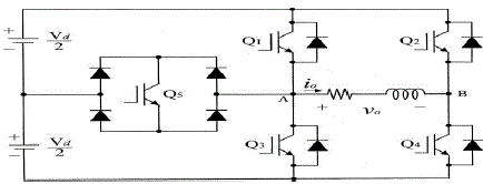
| Cascaded multilevel inverter has the advantage of most reliable and to achieve the best fault tolerance owing to its modularity; a feature that enables the inverter to continue operating at lower power levels after cell failure. Modularity also permits the cascaded multilevel inverter to be stacked easily for high power and high voltage applications. The cascaded multilevel inverter typically comprises several identical single phase H-bridge cells cascaded in series at its output side. This configuration is commonly referred to as a cascaded H-bridge (CHB), which can be classified as symmetrical if the dc bus voltages are equal in all the series power cells, or as asymmetrical if otherwise. The main disadvantage of the conventional cascaded H-bridge is that when the voltage level increases, the number of semiconductor switches increases and also the source required increases. In order to overcome this introduced a new topology of cascaded H-bridge. The main advantage of this topology is that the number of switches required is reduced and also the number of sources. Figure 1 shows the new cascaded five levels H-bridge multilevel inverter. It has additional one bidirectional switch connected between the first leg of the H-bridge and the capacitor midpoint, enabling five output voltage levels. |
| It has five output voltage levels i.e. Vdc, Vdc/2, 0, -Vdc/2, -Vdc. For getting the output voltage Vdc, the switches S1S4 need to be turned on. Similarly for output voltage Vdc/2 switches S5S4 need to be turned on, for 0 either S3S4 or S1S2 need to be turned on; for - Vdc/2 switches S5S2 need to be turned on; for - Vdc switches S3S2 need to be turned on. The switch combinations are shown in table 1. |
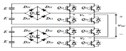
| In the circuit shown in fig 1, single H-bridge module is capable of producing five level output voltage. Each inverter module is capable of producing 2E, E, 0, -E, -2E. That means by using two bridges 9 level output voltage is produced. The total output voltage is sum of the outputs of the inverter modules and the nine voltage levels are 4E, 3E, 2E, E, 0, - E, -2E, -3E, -4E. The advantages of this proposed circuit is number of switches are reduced. The cost and complexity is less in this circuit. To synthesize nine output voltage levels, it employs two independent dc voltage sources of 2E which are divided into two input sources E in order to secure an additional dc voltage source of E. The inverter module having a bidirectional switch produces 5-levels of output voltage (- 2E, -E, 0, E, 2E) by controlling of the switches. Since every output terminal of the inverter module is connected in series, the output voltage becomes the sum of the terminal voltages of each inverter. The circuit for nine level cascaded H-bridges is shown in figure 2, the gating signals for the inverter is generated by using multicarrier modulation. |
PWM MODULATION
|
| In this inverter, the sinusoidal pulse width modulation is going to use. In the Sinusoidal pulse width modulation scheme, as the switch is turned on and off several times during each half-cycle, the width of the pulses is varied to change the output voltage. Lower order harmonics can be eliminated or reduced by selecting the type of modulation for the pulse widths and the number of pulses per half-cycle. Higher order harmonics may increase, but these are of concern because they can be eliminated easily by filters. The SPWM aims at generating a sinusoidal inverter output voltage without low-order harmonics. This is possible if the sampling frequency is high compared to the fundamental output frequency of the inverter. |
| The modulation index, M of the proposed multilevel inverter is defined by, |
 |
| Where Vref is the amplitude of the voltage reference and Vcr is the amplitude of the carrier signal. Multicarrier phaseshifted PWM (CPS-PWM) modulation is used to generate the PWM signals. The amplitude and frequency of all triangular carriers are the same as well as the phase shifts between adjacent carriers. Depending on the number of cells, the carrier phase shift for each cell, θcr,n can be obtained from, |
 |
| For signal generation in each cell, two voltage references and one carrier signal are used. Vref is defined by |
 |
 |
 |
| Both references are identical but displaced by an offset equal to the carrier’s amplitude which is ½. When the voltage reference is between 0<vref≤½, vref1 is compared with the triangular carrier and alternately switches S1 and S3 while maintaining S5 in the ON state to produce either ½vdc or 0. Whereas, when the reference is between ½<vref≤1, vref2 is used and alternately switches S1 and S2 while maintaining S5 in the ON state to produce either ½vdc or vdc. As for the reference between –½<vref≤0, vref1 is used for comparison which alternately switches S1 and S2 while maintaining S4 in the ON state to produce either –½vdc or 0. For a voltage reference between –1<vref≤–½, vref2 is compared with the carrier to produce either –½vdc or –vdc alternately switches S1 and S3, maintaining S4 in the ON state. It is noted that two switches, S4 and S5, only operate in each reference half cycle. This implies that both switches operate at the fundamental frequency while the others operate close to the carrier frequency. This allows the dc voltage to be switched at a low frequency so as to reduce the switching losses. Fig.3 shows the modulation scheme used for the proposed twocell configuration and Fig. 4 shows a detail block diagram for generating the PWM signals. |
SIMULATION RESULTS
|
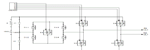
| The simulation model was designed using MATLAB/Simulink Software. The gating signals for the inverter are generated by using multicarrier pulse width modulation technique. The circuit was simulated with induction motor load. Figure 5 shows the circuit arrangement with multicarrier modulation. |
| The simulation result shows that THD gets reduced significantly when the output voltage level increases. |
HARDWARE IMPLEMENTATION
|
| The circuit has hardware implemented with induction motor as load. An 8-bit microcontroller AT89S8253 was used to generate the PWM signals. The inverter was supplied by a 12V battery supply. The modulation index was set to M = 0.8. The specification of each cell is given in Table 3. Of the 10 MOSFETs, 2 form the bi-directional switches. There are 4 dc capacitors, 8 diodes and 6 full-bridge rectifiers. |
| The output voltage obtained is 32V and it is stepped up to 230V to drive the induction motor. The experimental setup is shown in figure 18.The output voltage waveforms are shown in figure 19 and 20. |
CONCLUSION
|
| Multilevel inverters have become an effective and practical solution for increasing power and reducing harmonics of ac waveforms. This project deals with the design and implementation of single-phase nine-level Cascaded H-bridge multilevel inverter for induction motor load with multicarrier phase-shifted PWM modulation method. The simulation and hardware implementation of 9-level cascaded H-bridge was made. Along with it, its harmonic analysis was done. The simulation results shows that the developed nine-level Cascaded H-bridge Multilevel inverter has many merits such as reduce number of switches, lower EMI, less harmonic distortion and the THD obtained is 13.15%. The study of this topology can also be extended to three phase induction motor and also to reduce the number of switches. |
ACKNOWLEDGMENT
|
| Fore mostly, I would like to express my sincere gratitude to our Principal: Dr K. S.M Panicker, for his guidance. I am also thankful to our HOD Dr.Pailo Paul for imparting fundamental idea, which helped me a lot for my project. I am extremely thankful to my guide Mrs.Rebiya Rasheed for her guidance and suggestions; I would also like to thank all my teachers and my husband Mr.Veneesh C.S who gave their full support and encouragement for doing this project. I owe my deepest gratitude to them. |
Tables at a glance
|
|
|
| |
Figures at a glance
|
 |
 |
 |
 |
 |
| Figure 1 |
Figure 2 |
Figure 3 |
Figure 4 |
Figure 5 |
 |
 |
 |
 |
 |
| Figure 6 |
Figure 7 |
Figure 8 |
Figure 9 |
Figure 10 |
 |
 |
 |
 |
| Figure 11 |
Figure 12 |
Figure 14 |
Figure 15 |
 |
 |
 |
 |
 |
| Figure 16 |
Figure 17 |
Figure 18 |
Figure 19 |
Figure 20 |
|
| |
References
|
- NasrudinAbd. Rahim, MohamadFathiMohamad Elias, Wooi Ping Hew, IEEE transaction. Industry Electronics, “Design of filter to reduce harmonic distortion in industrial power system”, Vol. 60, No :8, 2943-2956, August 2013.
- J. Selvaraj and N. A. Rahim, "Multilevel Inverter For Grid-Connected PV System Employing Digital PI Controller," IEEE Trans. Ind.Electron., vol. 56, pp. 149-158, 2009.
- Naderi and A. Rahmati, "Phase-Shifted Carrier PWM Technique for General Cascaded Inverters," IEEE Trans. Power Electron.,vol. 23, pp. 1257-1269, 2008.
- J. Rodriguez, J.-S. Lai, and F. Z. Peng, ?Multilevel inverters: A survey of topologies, controls, and applications,? IEEE Trans. Ind. Electron., vol. 49, no. 4, pp. 724–738, Aug. 2002.
- M. Malinowski, K. Gopakumar, J. Rodriguez, and M. A. Pérez, ?A Survey on cascaded multilevel inverters,? IEEE Trans. Ind. Electron., vol. 57, no. 7, pp. 2197-2206, July 2010.
- S. J. Park, F. S. Kang, M. H. Lee, and C. U. Kim, ?A new single-phase five-level PWM inverter employing a deadbeat control scheme,? IEEE Trans. Power Electron., vol. 18, no. 18, pp. 831–843, May 2003.
- N. A. Rahim, and J. Selvaraj, ?Multistring five-level inverter with novel PWM control scheme for PV application,? IEEE Trans. Ind. Electron., vol. 57, no. 6, pp. 2111-2123, June 2010.
|