Keywords
|
| graphene, electronic properties, superlative, efficient, technological. |
INTRODUCTION
|
| Graphene is basically a thin layer of pure carbon ,it is tightly packed layer of carbon atoms which are bonded in a hexagonal lattice .It is till date the thinnest compound ,the lightest material known and the strongest compound discovered (between 100-300 times stronger than steel and tensile strength of 150,000,000 psi). Moreover the best conductor of heat at room temperature and also the best conductor of electricity known (electron mobility of more than 15,000 cm2v-1; s-1).It also has a tremendous property of absorbing white light .As its basically carbon, we already know the second most abundant mass in human body &fourth in universe, these all properties make it an ecologically friendly material. |
RELATED WORK: UNDERSTANDING WAFER SCALE GRAPHENE
|
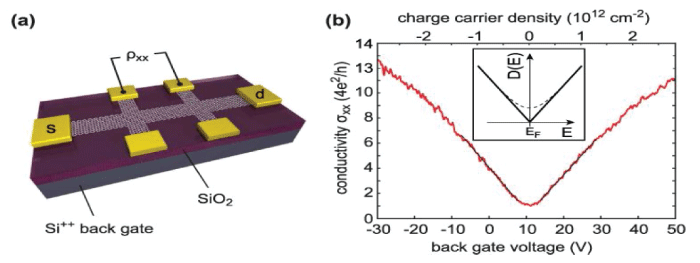
| Among all the different problems, the biggest problem is the difficulty in controlling charge transport .Today graphene can be manufactured both at wafer scales & beyond ,but scaled up samples show different structure to micrometre flakes ,which are usually crystalline in structure. Topological defects, line defects which separate 2D single crystalline domains are intrinsic to polycrystalline materials and have a significant impact on electronic properties of grapheme These defects basically affect the electronic transport properties of graphene. During transport charge carriers pass througha grain boundary with a certain probability this transmission probability varies according to many factors |
| 1) Energy of the charge carrier , |
| 2) On the direction it travels in respect to the grain boundary, |
| 3) Also on the characteristics of the grain boundary itself. |
| There can also be a phenomenon which is observed theoretically; grain boundaries of certain structural types completely reflect the charge carriers in certain energy ranges. |
USING DEFECTS
|
| These defects may be used as device components but these utilizing properties are not present in single crystalline graphene. These defects are difficult to study or to use them ironically, there is no such method of control over the structure of these defects developing such a method would require a high and competence level of engineering . |
EFFECTIVE PRODUCTION FROM ITS OXIDE
|
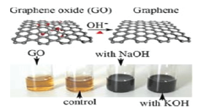 |
| Today graphene is normally produced using mechanical or thermal exfoliation, chemical vapour deposition (CVD), or epitaxial growth. The best method for production of graphene would be chemical reduction of graphene oxide, As people want cheaper, simple, more efficient & better methods of producing graphene. So chemical reduction method is used mostly. |
GRAPHENE PROPERTIES
|
| FUNDAMENTAL CHARACTERISTICS |
| Before 2004, when monolayer grapheme came into existence, till then it was believed that 2 dimensional compounds are impossible to exist because of thermal stability when separated. But, while graphene was isolated, it became clear that it was possible but the reason was unknown later, after some research it was found that this happened because carbon carbon bond in graphene are so small and strong that they prevent thermal fluctuation. |
| A. ELECTRONIC PROPERTIES |
 |
| The one of the bets properties of graphene, is that it is a zero-overlap semi metal (As is with both electron &holes asCharge carriers) with very high electrical Conductivity .Carbon has 6 electrons, 2 in inner and 4 in outer, the 4 outer shell electrons in an individual atom are available for chemical bonding but in case of graphene, each atom is connected to 3 other on the 2 dimensional plane, leaving 1 electron freely available in 3 dimensional for electronic conduction. These highly mobile electrons are called pie electrons and are located above & below graphene shed. Tests have shown that the electronic mobility of graphene is very high. It is said that graphene act very much like photons in this mobility due to lack of mass .These charge carriers are able to travel sub micrometer distance without scattering , a phenomenon called ballistic graphene used will be the limiting factors . |
| B. MECHANICAL STRENGTH |
| Another fascinating feature of this novel material is its inherent strength .Due to its strength of its 0.142Nm long Cbonds; graphene is the strongest material ever known ,has ultimate tensile strength of 130,000,000,000 Pascal compared to 400,000,000 for A 36 structure steel or 375,700,000 for Aramid (kelwar). Not only this material is the extraordinary strong but also every light at 0.77 milligrams per square sheet .some other things also add up with this material that is its elasticity being able to retain its initial size after strain .Tests were performed on graphene and was observed that it had spring constants in region of 1-5N/m & young’s modulus of 0.5Tpa again these superlative figures are based on the theoretical analysis. |
| C. OPTICAL PROPERTIES |
| Graphene has ability to absorb a rather large 2.3% of white light which is also a unique feature especially for an atom which is only 1 atom thick .It is proved earlier that the amount of white light absorbed depends upon fine structure constant rather than being dictated by material specifics .Adding another layer of graphene ,increases the amount of lightabsorbed by approximately the same value (2.3%).Due to these impressive properties , it is observed that once optical intensity reaches a certain threshold saturation absorption takes place .this is an important feature to mode locking of fiber lasers. Full band mode locking has been achieved using erbium doped dissipative solution fiber laser capable of obtaining wavelength tuning, as large as 30 nm. |
DIFFERENCE BETWEEN GRAPHITE AND GRAPHENE
|
| Graphene is basically one single layer of graphite; a layer of Sp2 bonded carbon atoms arranged in honeycomb lattice, Graphite another hand is a naturally a very brittle compound and cannot be used a structural material. Graphene is the strongest material ever known, 40 times stronger than diamond itself .Electrical conductivity of graphene is much higher than graphite due to the occurrence of free pie electrons for each carbon atom. |
GRAPHENE BASED SUPERCAPACITORS
|
| It can be seen that many kind of electrochemical batteries are being used for storage of charge and used in various applications but the limitation is that these batteries require a very long time to get charge , even the electric cars introduced these days require a charge of 31 hours to go for 250 km . On other hand, super capacitors are a good option, these capacitors can store hundred times more amount of charge than batteries, and moreover these super capacitors can work at very low temperatures and these are also being used in emergency radios and flash lights. The limiting factor with these super capacitors is that they cannot withstand high voltages i.e. maximum of 5 volts whereas electrochemical batteries can withstand hundreds of voltages. Firstly, Graphene is the upcoming material which can be instead of activated carbon, as is the surface area of graphene is substantially more than carbon. Secondly it is far lighter as it is made up of single atom layer. Thirdly and importantly the upper limit of graphene based super capacitors is 550 F/g which is far high. |
APPLICATIONS IN DIFFERENT INDUSTRIES
|
| 1) BIOLOGICAL ENGINEERING |
| The property that graphene shows that it could revolutionize this area in many ways as is it offers a large surface area , high electrical conductivity, thinness and strength it would be helpful in development of fast & efficient .Biometric sensory devices with monitory things as glucose levels, hemoglobin levels, cholesterol and even DNA sequencing. In future we may see engineered toxic graphene that can be used as an antibiotic or even anticancer treatment. |
| 2) OPTICAL ELECTRONICS |
| A particular area in which graphene would be soon seen is optoelectronics especially in touch screen, liquid crystal (LCD) and organic light emitting diodes. For a material to be used for optoelectronics it must have the ability to transmit more than 90 % of light &also offer high electricalconductivity to our fortune graphene is almost transparent up to 97.7% of light. |
| 3)ULTRAFILTRATION |
| Another unique property of this material while it allows water to pass through it, it is almost completely impervious to liquids and gases. This shows that graphene can be used as an ultrafiltration medium to act as barrier between two substances .As its benefit is that graphene is only 1 single atom thick and can also be developed as barrier that electronically measures strain and pressure between two substances. So graphene can be used in water filtration systems, desalination systems in future. |
| 4)AIRCRAFT INDUSTRY |
| As we know graphene is strong, stiff and very light currently aerospace engineering are using carbon fibre into production of aircraft as it is also very strong and light both.However graphene shows more strong ness and much lighter so it can be seen in future industries that graphene could replace steel and reduce the efficiency, range and reduce weight .Due to its electrical conductivity it can also be used to coat the outer surface of aircrafts to prevent electric damage from lightening, same coating could also help the pilot to notify any change in stress levels that the aircraft wings undergo, measure strain rate. |
| 5)PHOTOVOLTAIC CELL |
| Photovoltaic cells are usually made up of silicon, but these silicon cells are very expensive to produce, graphene based cells are potentially much less .As materials like silicon convert light into electricity it produces a photon for every electron, resulting as heat, whereas in case of graphene it has been observed that when it absorbs photon, it releases multiple electrons .Secondly silicon can convert only certain wavelength bands whereas graphene works on all wavelengths. In future due to its flexibility graphene based photovoltaic cells could be used in clothing to recharge your phones or as curtains of window screen to supply power to house. |
| CONCLUSION |
| We finally observe that graphene is material which possesses novel electronic properties, and could be used in future for many other aspects also, other than discussed here. Although scientists are finding many problems with its high production costs but many researchers are still experimenting news ways for its efficient production. |
References
|
- One of possible models for the complex graphene-SiC interface is given by S. Kim, J. Ihm, H. J. Choi, Y.W. Son, Phys. Rev. Lett. 100, 176802 (2008).
- W. J. Beenakker, H. van Houten, Semiconductor Heterostructures and Nanostructures, in H. Ehrenreich, D. Turnbull (Eds.) (Academic Press, New York, 1991).
- J. O. Sofo, A. S. Chaudhari, G. D. Barber, Phys. Rev. B 75, 153401 (2007).
- X. Wang, L. Zhi, K. Müllen, Nano Lett. 8, 323 (2008); there are several other reports on the same subject, which appeared later in 2008.
- Nair, R. R.; Wu, H. A.; Jayaram, P. N.; Grigorieva, I. V.; Geim, A. K. (2012). "Unimpeded permeation of water through helium-leak-tight graphene-based membranes"
- Nalla, Venkatram; Polavarapu, L; Manga, KK; Goh, BM; Loh, KP; Xu, QH; Ji, W (2010). "Transient photoconductivity and femtosecond nonlinear optical properties of a conjugated polymer–graphene oxide composite"
- Whitby, Raymond L.D.; Korobeinyk, Alina; Glevatska, Katya V. (2011). "Morphological changes and covalent reactivity assessment of singlelayer graphene oxides under carboxylic group-targeted chemistry".
- Neto, A Castro; Peres, N. M. R.; Novoselov, K. S.; Geim, A. K.; Geim, A. K. (2009). "The electronic properties of graphene"
- Lenski, Daniel R.; Fuhrer, Michael S. (2011). "Raman and optical characterization of multilayer turbostraticgraphene grown via chemical vapor deposition". Journal of Applied Physics.
- "New process could lead to more widespread use of graphene". Gizmag.com. Retrieved 2014-06-14.
- gigaom.com/.../what-is-graphene-heres-what-you-need-to-know-about-by Signe Brewster - Jul 15, 2013.
- Bao, Qiaoliang; Zhang, Han; Wang, Yu; Ni, Zhenhua; Yan, Yongli; Shen, Ze Xiang; Loh, Kian Ping; Tang, Ding Yuan (2009). "Atomic-Layer Graphene as a Saturable Absorber for Ultrafast Pulsed Lasers"
- Zhang, H.; Tang, D. Y.; Zhao, L. M.; Bao, Q. L.; Loh, K. P. (2009). "Large energy mode locking of an erbium-doped fiber laser with atomic layergraphene"
- Geim, A. K.; Novoselov, K. S. (2007). "The rise of graphene". Nature Materials 6 (3): 183–91.
- "Graphene Uses & Applications". Graphenea.Retrieved 2014-04-13.
- "Samsung's graphene breakthrough could finally put the wonder material into real-world devices". ExtremeTech. 2014-04-07. Retrieved 2014- 04-13.
- Graphene/carbon nanotube hybrid supercapacitors by Dingshang Yu of Nanyang Technological University in Singapore and Case Western’s and Laming Dai, who are also members of the current international research team (China is also participating, through Tsinghua University).
- DOI:10.1126/science.1239089 – “Liquid-Mediated Dense Integration of Graphene Materials for Compact Capacitive Energy Storage”.
|