Keywords
|
| MSPWM, multilevel inverter, coupled inductors |
INTRODUCTION
|
| MULTILEVEL inverters (MLIs) are finding increased attention in industries as a choice of electronic power conversion for medium voltage and high-power applications, because improving the output waveform of the inverter reduces its respective harmonic content and hence, the size of the filter used and the level of electromagnetic interference generated by switching operation. The output of conventional two-level inverter is in the form of square wave ac power which usually contains undesirable harmonics. When this output is fed to an electrical device such as an electrical motor it causes heating which in turn causes increased losses and finally resulting in decreased efficiency. This is caused by high harmonic contents. These harmonics increases the total harmonic distortion value which is responsible for reducing the quality of output. The harmonics has to be removed in order to attain a proper sine wave. The harmonics in the output side of the inverter can be eliminated using multi level inverter structures |
| MLIs can operate by MSPWM techniques such as Alternate phase opposition and disposition(APOD),Phase Opposition and Disposition(POD), Phase disposition(PD). combination of Fundamental Switching Frequency Modulation (FPWM) and High Switching Frequency Modulation MSPWM for each inverter cell operation. Most of the modulation methods developed for MLI is based on multiple-carrier arrangements with pulse width modulation (PWM).The carriers can be arranged with vertical shifts (PD, POD,APOD) or with horizontal displacements (phaseshifted carrier (PSCPWM). |
| For single-phase multilevel inverters, the most common topologies are the cascaded, diode-clamped, and capacitor clamped types . In general, multilevel inverter topologies can be classified into two types: Type I and Type II. Type I uses multiple dc voltage sources and Type II uses multiple (split or clamping) dc voltage capacitors. Type I includes the traditional cascaded topologies , those presented in and so forth. Type II includes the conventional diodeclamped, capacitor-clamped inverters, the topologies proposed in. In terms of single phase multilevel inverters, the disadvantages of the two types are apparent. Type I suffers from the availability of the multiple dc voltage sources. In practice, bulky transformers either of low or medium frequency are usually necessary if a Type I inverter is adopted. This is a great challenge to when it comes to volume ,weight, and cost minimization. The problem with Type II is mainly the balancing of the dc capacitor voltages, though some topologies can achieve self-balancing with certain control algorithms. |
LITERATURE SURVEY
|
| Zixin Li, Ping Wang, Yaohua Li, and Fanqiang Gao [1] perform analysis on Multilevel inverters are finding in increased attention in industries as a choice of electronic power conversion for low to medium power applications that too for high current cases.J.Rodriguez,S.Bernet,B.Wu,J.O.Pontt and S.Kouro(2007) [1] perform analysis on MULTILEVEL inverters (MLIs) are finding increased attention in industries as a choice of electronic power conversion for medium voltage and high-power applications, because improving the output waveform of the inverter reduces its respective harmonic content and, hence, the size of the filter used and the level of electromagnetic interference (EMI) generated by switching operation.M.Malinowski, K. Gopakumar, J. Rodr´Ãâñguez, andM. A. Perez (2010) [3] presented a bibliographical review of cascaded multicell inverters, its working principle, circuit topologies, control techniques, and industrial applications. Nowadays, there exist three commercial topologies of multilevel voltage-source inverters: neutral point clamped (NPC), cascaded H-bridge (CHB) , and flying capacitors (FCs) . Among these inverter topologies, cascaded multilevel inverter reaches the higher output voltage and power levels (13.8 kV, 30 MVA) and the higher reliability due to its modular topology. In the case of a fault in one of these modules, it is possible to replace it quickly and bypass the faulty module without stopping the load, bringing an almost continuous . |
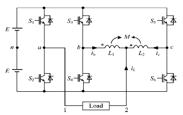
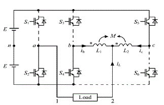
| This paper presents a single-phase five-level inverter using coupled inductors and the common three-arm power module shown in Fig.1[1]. With the proposed inverter, only one dc voltage source is needed and split of the dc voltage capacitor is also avoided, which eliminates the problem of dc capacitor voltage balancing with the conventional topologies. Meanwhile, six power switches with the same voltage stress and only one set of coupled inductors are adopted. Also, less inductor is needed in the inverter proposed .In addition, the simulation results for all the MSPWM scheme for this inverter is also presented. With these modulation methods, no dc component exists in the inductor currents under all load conditions, which will benefit the full use of the magnetic cores and minimization of the inductors. Theoretical analyses, numerical simulation, and experimental results are presented to show the validity of the proposed inverter with the optimized modulation method. |
Role of the Coupled Inductors
|
| It is, in fact, the adoption of the coupled inductors that makes it possible to output five level voltage with only one dc voltage source. So the role of the coupled inductors will be analyzed first. Suppose that the two coupled inductors are with the same number of turns or obtained by a center-tapped inductor. The leakage inductances of the two inductors are Lσ1 and Lσ2 , respectively. Assuming that Lσ1 = Lσ2 = Lσ , the voltage equations of the coupled inductors can be expressed as follows: |
 |
 |
| Meanwhile, according to Kirchhoff’s current law, one can obtain |
 |
| From (1) to (3), the following equation can be derived |
 |
| Generally, the leakage inductance can be designed to be very small and its influence can be ignored in most cases. Therefore,(4) can be rewritten as |
 |
| This result shows that the coupled inductors will perform as an adder of the two input voltage at the noncommon- connected terminals with the common-connected terminal as the output. Actually, without the help of the coupled inductors, the proposed inverter will not be able to output five-level voltage. |
MODES OF OPERATION
|
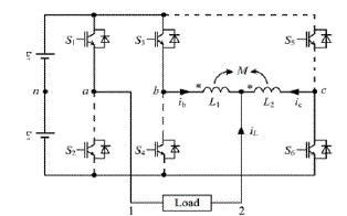
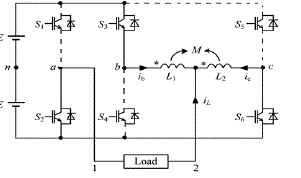
| In this case, the voltage of u12 should alternate between +2E and +E. According to Table I, the switching states of (S3 , S5 ) within every switching period the output has to change from (0,0) to (0,1) or (0,0) to (1,0) defined as mode 1. |
| Mode 2: LEVEL E |
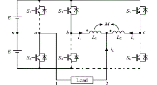
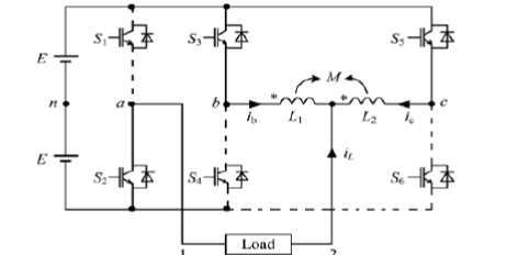
| In this occasion, the voltage of u12 should alternate between +E and 0. Based on Table I, the switching states of (S3 , S5 ) within every switching period the output has to change from (1,1) to (0,1) or (1,1) to (1,0) defined as mode 2 . |
| Mode 3: LEVEL -E |
| In this occasion, the voltage of u12 should alternate between -E and 0. Based on Table I, the switching states of (S3 , S5 ) within every switching period the output has to change from (1,1) to (0,1) or (1,1) to (1,0) defined as mode 2 when S1=0 . |
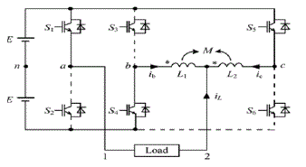
| LEVEL -2E: |
| In this occasion, the voltage of u12 should alternate between -E and 0. Based on Table I, the switching states of (S3 , S5 ) within every switching period the output has to change from (1,1) to (0,1) or (1,1) to (1,0) defined as mode 2 when S1=0. |
| From Fig.1 , the output voltage of the proposed inverter can be expressed as |
| In the following discussion, the power switches in one arm are assumed to switch complementarily. For instance, S2 must be turned OFF if S1 is turned ON and vice versa. So the following discussion will only focus on the switching states of S1 , S3 , and S5 . For convenience of analysis, the number 1 will be used to denote the ON state of one switch and 0 will be used to denote the OFF state. In fact, u1n,u2n all can generate two level voltage (+E and −E). According to (6), the voltage levels of u12 can be summarized in Table I. Obviously, the proposed inverter can generate five voltage levels at its output terminals. From Table I, it should be pointed out that the switching state of S1 must be 1 if u12 ≥ 0 and the switching state of S1 must be 0 if u12 ≤ 0. This means S1 and S2 will switch at the fundamental frequency of the reference signal. So, the switching losses of S1 and S2 will be very low in the proposed inverter. |
CONTROL TECHNIQUE OF FIVE LEVEL INVERTER
|
| From the above analysis, the switching state of S1 is decided by the sign of u12ref (the reference of u12): S1 is 1 if u12ref ≥ 0 and S1 is 0 if u12ref ≤ 0, which is very easy to implement. However, the switching states of S3 and S5 cannot be selected without careful study. |
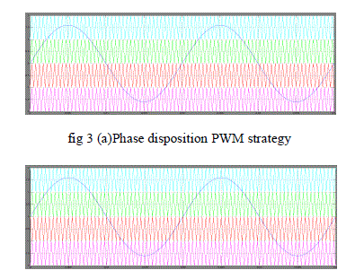
| Although the proposed inverter can output five-level voltage, the modulation method must be analyzed in detail for safe operation. This section will focus on the pulse-width modulation (PWM) methods for the multilevel inverters. This work used the intersection of a sine wave with a triangular wave to generate firing pulses for a five level inverter. Most carrier-based PWM schemes for multilevel inverters derive from the carrier disposition strategy presented by Carraraet al. []. For an N -level inverter, this strategy arranges triangular carriers with the same frequency and amplitude so that they fully occupy contiguous bands over the range to . A single sinusoidal reference is then compared with each carrier to determine the switched output voltages for the converter. Three alternative carrier disposition PWM strategies are commonly referenced, |
| a. Phase disposition(PD) PWM strategy. |
| b. Phase opposition disposition(POD) PWM strategy. |
| c. Alternate phase opposition disposition(APOD) PWM strategy. |
| The following formula is applicable to sub-harmonic PWM strategy i.e. PD, POD and APOD. |
| The frequency modulation index |
 |
| where, |
| mf = frequency modulation index |
| fc = frequency of carrier (Hz) |
| fm = frequency of reference(Hz) |
| The amplitude modulation index |
 |
| where, |
| ma = amplitude modulation index |
| Am = amplitude of the reference signal (V) |
| Ac = amplitude of the carrier signal(V) |
| m = number of levels |
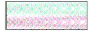
| Figures show the waveforms based on three schemes of level shifted multilevel modulations. |
| (a) in phase disposition (PD) , where all carriers are in phase; (b) alternative phase opposition disposition (APOD), where all carriers are alternatively in opposite disposition; and (c) phase opposite disposition (POD) , where all carriers above zero reference are in phase but in opposition with those below the zero reference. |
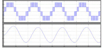
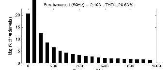
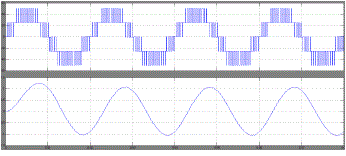
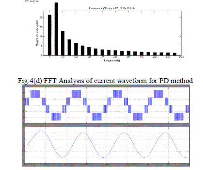
| In this work the simulation results of single phase five level inverter with coupled inductor various modulating strategies are obtained through MATLAB/SIMULINK. The output quantities like phase voltage, THD spectrum for phase voltage are obtained. It is observed that PODPWM method provides output with relatively low distortion. |
SIMULATION RESULTS
|
| The five level inverter parameters for the sample system are summarized in TABLE II . |
| For the multi level inverters for n level we have to use n-1 carrier signals with one reference signal. Since it is a five level inverter, four carrier waveforms are used. |
| From the above simulation the following results are obtained. |
 |
CONCLUSION
|
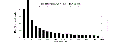
| From the above simulations it is evident that the APOD method has less THD when compared to other two methods. Then APOD method is the best method for this five level inverter. So, the closed loop has been done using APOD method. |
Tables at a glance
|
|
|
Figures at a glance
|
 |
 |
 |
 |
 |
| Figure 1 |
Figure 2a |
Figure 2b |
Figure 2c |
Figure 2d |
 |
 |
 |
 |
 |
| Figure 2e |
Figure 2f |
Figure 3 |
Figure 3c |
Figure 4a |
 |
 |
 |
 |
| Figure 4b |
Figure 4c |
Figure 4e |
Figure 4f |
|
| |
References
|
- Zixin Li, Ping Wang, Yaohua Li, and FanqiangGao, "A Novel Single-Phase Five-Level Inverter With Coupled Inductors", IEEE Trans. onPower Electronics,Vol.27, no. 6,pp.2716-2724, June 2012
- J. Rodriguez, J.-S. Lai, and F. Z. Peng, “Multilevel inverters: A Survey of topologies, controls, and applications,” IEEE Trans. Ind. Electron.,vol.49, no. 4, pp. 724–738, Aug. 2002.
- G.-J. Su, “Multilevel dc-link inverter,” IEEE Trans. Ind. Appl., vol. 41,no. 3, pp. 848–854, May 2005.
- D. Floricau, E. Floricau, and G. Gateau, “New multilevel converters with coupled inductors: Properties and control,” IEEE Trans. Ind. Electron.,vol. 58, no. 12, pp. 5344–5351, Jul. 2011.
- Brendan Peter McGrath and Donald Grahame Holmes, "Multicarrier PWM strategies for multilevel inverters" IEEE trans.Ind.Electron, Vol. 49,no.4,pp. 858-867, Aug. 2002.
- J. Salmon, A. Knight, and J. Ewanchuk, “Single phase multi-level PWM inverter topologies using coupled inductors,” in Proc. IEEE PowerElectron.Spec. Conf. (PESC), 2008, pp. 802–808.
- Ned Mohan, T.M.Undeland and William P. Robbins , “Power Electronics: Converters, Applications, and Design” Second Edition, 1995.
|