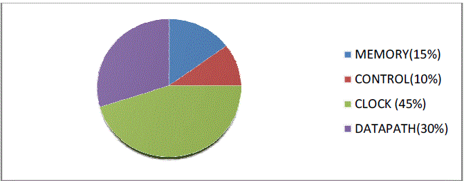
Power consumption has emerged as a principle theme in today’s widely and frequently used portable electronics. The datapath consumes roughly 30% of the total power of a modern day high performance microprocessor. Adders are key components used in datapaths and, therefore, careful design and analysis is required for these units to obtain optimum performance So the full adder designs with low power characteristics are becoming more popular these days. This paper presents a novel low power, energy efficient full adder circuit implementation for ultra deep submicron design. With rapid technology scaling, the main focus in low power design is targeted to reduce the static power while trading other vital requirements such as driving capability, delay, total power and noise immunity. Based on the fact that transmission logic has good driving capability and full signal swing than pass transistor logic, a new full adder cell is proposed to reduce delay and power-delay product (PDP).The simulations have been carried out with TANNER EDA simulation tool using PTM 65nm technology files. Simulations have been carried out for different supply voltages and loading conditions to compare the performance of the proposed circuit with respect to the existing ones.
Keywords |
| Novel, Low-Power, Energy-Efficient, Full Adder, ultra deep-Submicron. |
INTRODUCTION |
| The demand and and popularity of portable electronics is driving designers to strive for smaller silicon area, higher
speeds, longer battery life, and more reliability. Power is one of the premium resources a designer tries to save when
designing a system. Full adders are fundamental units in various circuits, especially in circuits used for performing
arithmetic operations such as compressors, comparators, parity checkers, and so on [1]. Full adders are often used in the
critical paths of complex arithmetic circuits for multiplication and division. These in turn form the core of any system
and thereby influence the overall performance of the entire system. Enhancing the performance of the full adder can
significantly affect the system performance. Figure 1 shows the power consumption breakdown in a modern day highperformance
microprocessor [2]. The datapath consumes roughly 30% of the total power of the system. Adders are an
extensively used component in datapaths and, therefore, careful design and analysis is required for these units to obtain
optimum performance. At the circuit level, an optimized design is desired to avoid any degradation in the output
voltage, consume less power, have less delay in critical path, and be reliable even at low supply voltage as we scale
towards deep sub micrometer. Good driving capability under different load conditions and balanced output to avoid
glitches is also an important virtue. Several logic styles have been proposed in the literature [1-12] to design 1-bit full
adder cell. Each design has its own merits and demerits in terms of output signal swings, driving capabilities, speed,
power, switching activity, noise immunity and so on. Generally, the focus in deep submicron technology is to reduce
the static power by replacing nMOS with pMOS transistors [12] or by stacking effect or by reducing the transistor
count [11]. In designing so, the designers often trade for other vital requirements such as area, driving capability, delay,
total power and noise immunity. The performance of such a full adder cell as a single unit is good but when these cells
are used as a building block of complex circuits, the performance degrades drastically. |
| In this paper, we presented an optimized design for a full adder cell craved for low power, low energy, reliable
operation at low supply voltage, avoiding degradation in the output voltage, good driving capability under different
loading conditions. The rest of the paper is organized as follows. In section II,a survey of contemporary literature on
full adders designs is presented. In section III, general overview of full adder with its sub modules is presented. In
section IV, the circuit for module II is proposed and combination of module II and III is presented. Using the proposed
combination in Section IV, we build a new full adder cell in Section V. Simulation results are presented in Section VI.
Section VII concludes the paper. |
LITERATURE REVIEW |
| A survey of contemporary literature reveals a wide spectrum of adder designs over the past few decades. Several
logic styles have been used in the past to design full adder cells. Each design style has its own merits and
demerits.Classical designs of full adders normally use only one logic style for the whole full-adder design. One
example of such design is the standard static CMOS full adder [3]. This full adder is based on regular CMOS structure
with conventional pull-up and pull-down transistors providing full-swing output and good driving capabilities. The
main drawback of static CMOS circuits is the existence of the pMOS block, because of its low mobility compared to
the nMOS devices. Therefore, the pMOS devices need to be sized up to attain the desired performance. The input
capacitance of a static CMOS gate is large because each input is connected to the gate of at least a pMOS and a nMOS
device This is another reason for speed degradation of static CMOS gates. Another conventional adder is the
complementary pass-transistor logic (CPL) [3]. It provides high-speed, full-swing operation and good driving
capability due to the output static inverters and the fast differential stage of cross-coupled pMOS transistors.But due to
the presence of a lot of internal nodes and static inverters, there is large power dissipation. The layout of a CPL cell is
also not as straightforward as a static CMOS cell due to its irregular transistor arrangement. The dynamic CMOS logic
style provides a high speed of operation because the logic is constructed with only high mobility nMOS transistors.
Also, due to the absence of the pMOS transistors, the input capacitance is also low, thus enhancing the speed of
operation. However, it has several inherent problems such as charge sharing and high clock load. It has higher
switching activity and lower noise immunity. It consumes a large portion of the power in driving the clock lines.
Moreover, dynamic logic style is more susceptible to leakage. Due to these reasons, we do not include dynamic logic
style in our discussions in this paper. |
| Some other full-adder designs include transmission-function full adder (TFA) [4] and transmission-gate full adder
(TGA) [5].These designs are based on transmission-function theory and transmission gates, respectively. These adders
are inherently low power consuming. These logic styles are good for designing XOR or XNOR gates. The main
disadvantage of these logic styles is that they lack driving capability. This is attributed to the fact that the inputs are
coupled to the outputs. When TGA or TFA are cascaded, their performance degrades significantly. |
| The remaining adder designs use more than one logic style for their implementation. We call this the hybrid-CMOS
logic design style. Examples of adders built with this design style are DB cell [6], NEW14-T adder [7], and hybrid pass
logic with static CMOS output drive full adder [8] (we will use HPSC as an abbreviation) and new-HPSC [9] adder.
These designs exploit the features of different logic styles to improve upon the performance ofthe designs using single
logic style. All hybrid designs use the best available modules implemented using different logic styles or enhance the
available modules in an attempt to build a low power full-adder cell. Generally, the main focus in such attempts
is to reduce the numbers of transistors in the adder cell and, consequently, reduce the number of power dissipating
nodes. This is achieved by utilizing intrinsically low power consuming logic styles like TFA or TGA or simply passes
transistors. In doing so, the designers often trade off other vital requirements such as driving capability, noise
immunity, and layout complexity. Most of these adders lack driving capabilities as the inputs are coupled to the
outputs. Their performance as a single unit or in small chains is good but when large adders are built by cascading these
1-b full-adder cells, the performance degrades drastically. |
FULL ADDER COMPONENTS |
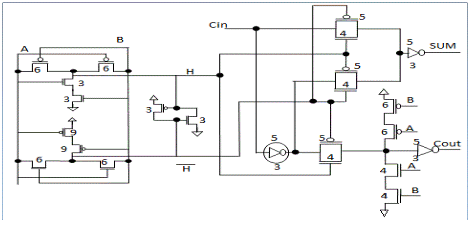
| A full adder can be broken down into three modules by extracting the logical expression for the outputs SUM and
Cout using the binary inputs A, B and Cin [1-12] as shown in figure 2. Module I essentially perform the XOR(H) and
XNOR(~H) functions in terms of the inputs A and B. In [6], the circuit for module I uses ten transistors and performs
well at low supply voltages. We consider this circuit for module I in our design. Module II and III generates SUM,
Cout respectively using three signals Cin, H and ~H as inputs. |
PROPOSED CIRCUIT FOR MODULE II |
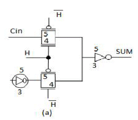
| The expression for output of module II can be expressed as SUM = Cin·H+ ~Cin · ~H. The proposed circuit for
module II is shown in Figure 2(a). A transmission gate followed by a static inverter at the output is used to implement
Cin·H. A transmission gate preceded and succeeded by static inverter implements ~Cin· ~H. Only one among the two
transmission gates is ON and the other is OFF at any time. The inverter (enclosed in circle in Figure 2) can be shared
between proposed module II and module III in [10], as shown in Figure 2(b). |
PROPOSED FULL ADDER CELL |
| In this section, we will present the new full adder design based on the circuits discussed in Section II and III .In our
proposed circuit, a single static inverter is shared to drive the transmission gates of both the modules II and III. At any point of time, only one among the two transmission gates driven by the inverter common to modules II and III are ON
and the other is OFF. The compliment of Cin is propagated in module III when H is at logic ‘1’ and ~H is at logic ‘0’.
In the other case, when H is at logic ‘0’ and ~H is at logic ‘1’, the compliment of Cin is propagated in module II. The
additional inverter for module II reduces the loading effect on H and ~H signals and speeds up the circuit in module II
to generate the SUM output. |
SIMULATION RESULTS |
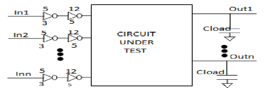
| All the circuits are simulated in TANNER EDA using PTM [13] 65nm technology model files. The simulation test
bench along with transistor sizes of each buffer is shown in Figure 4. The performance of the circuit is evaluated in
terms of the worst-case delay, power consumption and PDP for supply voltages 1.1V and 0.9V at 250 MHz frequency.
A change in the input may or may not lead to change at the output. As a result, some internal node may be switching
even if there is no switching at the output, this leads to some power consumption. All the possible input combinations
are taken in to account for an accurate result. |
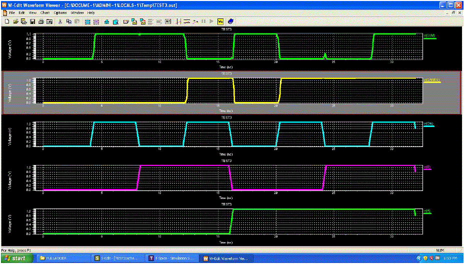
| Figure 5 shows input stimulus for a full-adder cell. The first two are outputs and the remaining three are inputs.
Frequency of the inputs is 250 MHz with a supply voltage of 1.1 V and output load CL=2.5fF.The value of worst case
delay and average power dissipated is evaluated under different supply voltages and different load conditions. The PDP
is a quantitative measure of the efficiency of the tradeoff between power dissipation and speed, and is particularly
important when low-power operation is needed. The values of PDP is evaluated under different supply voltages and
different output loads and the proposed adder showed a huge improvement as suggested by the simulation results. |
| Table I and Table II shows the comparison of full adders at different supply voltages and for different values of load
capacitance CL. The proposed adder full adder showed a good improvement in terms of power and delay when
compared to adder in [9] and [10] at the cost of increase in static power |
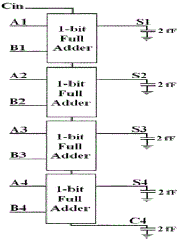
| We embedded our full adder cell in carry ripple (RCA) 4-bit full adder circuit to evaluate it in a realistic operating
conditions. The 4-bit full adder test circuit is shown in Figure 6. |
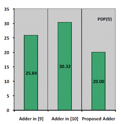
| The power- delay product(PDP) , figure of merit correlated with energy efficiency results of a 4 bit ripple carry
adder (RCA) at Vdd=1.1V,CL=2Ff and Frequency=50Hz are presented in figure 7. As shown in the figure proposed 4-bit
ripple carry (RCA) consumes less energy when compared with adder in [9] and [10]. The observations for PDP from figure 7
show 22% improvement when the simulation results are compared to its best counterparts. |
CONCLUSION |
| The simulation results show that the full adder is suitable for applications in ultra deep-submicron technologies. It
provides better delay and energy characteristics and performs well at different supply voltages and loading conditions,
making it suitable building block for complex circuits to be used in a dynamic voltage and frequency scaling (DVFS)
scenario. |
Tables at a glance |
 |
 |
| Table 1 |
Table 2 |
|
Figures at a glance |
 |
 |
 |
 |
| Figure 1 |
Figure 2 |
Figure 3 |
Figure 4 |
 |
 |
 |
| Figure 5 |
Figure 6 |
Figure 7 |
|
References |
- H.T.Bui, Y.Wang, and Y. Jiang, âÃâ¬ÃÅDesign and analysis of low power 10-transistor full adders using XORâÃâ¬ÃâXNOR gates,âÃâ¬Ã IEEE Trans. Circuits Syst. II, Analog Digit. Signal Process. vol. 49, no. 1, pp. 25âÃâ¬Ãâ30, Jan.2002
- V. Tiwari, D. Singh, S. Rajgopal, G. Mehta, R. Patel, and F.Baez,âÃâ¬ÃÅReducing power in high-performance microprocessors,âÃâ¬Ã in Proc. Conf. Des. Autom. 1998, pp. 732-737
- R. Zimmermann and W. Fichtner, âÃâ¬ÃÅLow-power logic styles: CMOS versus pass-transistor logic,âÃâ¬Ã IEEE J. Solid-State Circuits, vol. 32, July 1997, pp.1079âÃâ¬Ãâ90
- N. Zhuang and H. Wu, âÃâ¬ÃÅA new design of the CMOS full adder,âÃâ¬Ã IEEE J. Solid-State Circuits, vol. 27, no. 5, pp. 840âÃâ¬Ãâ844, May 1992
- N.Weste and K. Eshraghian, âÃâ¬ÃÅPrinciples of CMOS VLSI design,âÃâ¬Ã in A System Perspective. Reading, MA: Addison-Wesley, 1993
- Shams,A.M,.; Darwish, T.K.;Bayoumi, M.A.;, "Performance analysis of low-power 1-bit CMOS full adder cells," Very Large Scale Integration (VLSI) Systems, IEEE Transactions on, vol.10, no.1, pp.20-29, Feb 2002
- Radhakrishna, D.; "Low-voltage low-power CMOS full adder," Circuits, Devices and Systems, IEE Proceedings - , vol.148, no.1, pp.19-24, Feb 2001.
- M. Zhang, J. Gu, and C. H. Chang, âÃâ¬ÃÅA novel hybrid pass logic with static CMOS output drive full-adder cell,âÃâ¬Ã in Proc. IEEE Int. Symp. Circuits Syst., May 2003, pp. 317âÃâ¬Ãâ320.
- Chip-Hong Chang; JiangminGu; Mingyan Zhang; , "A review of 0.18Ãâõm adder performance for tree structured arithmetic circuitsâÃâ¬Ã Very Large Scale Integration (VLSI) Systems, IEEE Transactions on, vol.13no.6, pp. 686- 695, June 2005.
- Goel, S.; Kumar, A.; Bayoumi, M. A.; , "Design of Robust, Energy-Efficient Full Adders for Deep-Sub micrometer Design Using Hybrid- CMOS Logic Style," Very Large Scale Integration (VLSI) Systems, IEEE Transactions on, vol.14, no.12, pp.1309-1321, Dec. 2006
- Fayed, A.A.; Bayoumi, M.A.;, "A low power 10-transistor full adder cell for embedded architectures," Circuits and Systems, 2001. ISCAS 2001. The 2001 IEEE International Symposium on, vol.4, no., pp.226-229 vol. 4, 6-9 May 2001.
- Weiqiang Zhang; Linfeng Li; Jianping Hu; , "Design techniques of P Type CMOS circuits for gate-leakage reduction in deep sub-micron ICs," Circuit and Systems 2009.MWSCAâÃâ¬Ãž09.52nd IEEE International Midwest Symposium on, vol., no., pp.551-554, 2-5 Aug.2009.
- Predictive technology model currently available online at www.eas.asu.edu/~ptm.
|