Comparator is one of the most widely used building block for analog and mixed signal systems. For the implementation of high-performance CMOS A/D converters, low offset comparators are essential. In this paper, dynamic comparator offset is calculated to the extent of high accuracy. The offset so calculated has been reduced by the charge storage techniques to achieve an efficient design. In addition to the offset, propagation delay and power dissipation, being the important parameter of the comparator, has been analyzed. It is observed that offset voltage in the comparator has been reduced to 350μV for output offset storage technique and 400μV for input offset storage techniques from 91mV. In this paper, BPTM model has been used in analyze the dynamic comparator.
Keywords |
| Dynamic comparator, offset voltage, storage capacitor, input offset storage, output offset storage. |
INTRODUCTION |
| A comparator is essential component of an ADC. A comparator compares a differential input signal with a predetermined
threshold voltage and gives a digital decision accordingly [1]. The major portion of the total power consumption results
from the static power dissipated in analog circuit components that require DC bias currents. One efficient method is to use a
dynamic comparator. In this way the static power consumption can be reduced. But at the expense of high offset error.
Because such comparator topologies do not have static pre-amplification in the front of a latch part, thus have unavoidably
large offset voltages. |
| The offset of a comparator can be defined by additional differential input signal to the ideal differential input to achieve a
desired output [2]. Offset voltage affects the accuracy of the circuit. In order to achieve an optimum comparator design, it is
essential to have accurate methods to predict offset voltages. |
| In this work, Section 2 describes the brief introduction about preamplifier based dynamic comparator. Section 3 presents
the offset voltage minimization techniques. Section 4 deals with the results and discussions. Finally the section 5 offers the
brief conclusion. |
PREAMPLIFIER BASED DYNAMIC CMOS COMPARATOR |
| Device mismatch results in an input referred offset for the latch as a result of threshold voltage, W/L, and μCox variations
[3]. Therefore, the latch must be preceded by a circuit that amplifies the (VIN - VREF) difference before it is applied to the
latch. This amplifier circuit must have a large enough gain so that the minimum difference signal to be resolved is amplified
to a voltage large enough to overcome the input referred offset of the latch [4]. |
| Fig. 1 shows the block diagram of a pre-amplifier based dynamic CMOS comparator. It consists of the two stages viz. preamplifier
and latch. Preamplifier circuit is a differential amplifier with active loads. The output currents of the preamplifier
are mirrored into the latch stage. The latch stage consists of a cross-coupled pair of NMOS and PMOS transistors.
In this preamplifier based comparator circuit offset is stored and canceled without adding any extra timing overhead by
using input offset storage (IOS) and output offset storage (OOS) techniques. |
OFFSET CANCELLATION TECHNIQUES |
| The analog sampling capability inherent in CMOS and BICMOS technologies provides a means whereby offsets can be
periodically sensed, stored, and then subtracted from the input [5]. Both of the offset cancellation topologies i.e. IOS and
OOS comprise a preamplifier, offset storage capacitor, and a regenerative latch. With IOS, the cancellation is performed by
closing a unity-gain loop around the preamplifier and storing the offset on the input coupling capacitors. With OOS, the
offset is cancelled by shorting the preamplifier inputs and storing the amplified offset on the output coupling capacitors.
Both circuits are driven by a clock. The two-phase non overlapping clocking used to operate the circuits. |
| A. Input offset storage (IOS) |
| Fig. 2 shows the application of input offset storage (IOS) technique to the dynamic comparator consists of a preamplifier,
offset storage capacitors (Cs) and a latched comparator. Cp is the parasitic capacitance at each charge observation node,
which includes the input capacitance of the pre-amplifier, parasitic capacitance at the drain of the transistors in switches
S3a/S3b, and the capacitance of the metal interconnects. |
| The comparator examines the input in ph2 – normal operation. Reference voltages are applied to the capacitors during ph1
which is the offset sampling phase. During this phase, the switches S2a/S2b/S3a/S3b turn on, resettling the input and closing a
unity gain loop around the preamplifier. In this situation its differential input voltage, |
 |
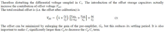 |
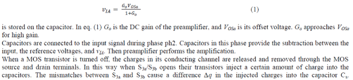
| B. Output Offset Storage (OOS) |
| Fig. 3 shows the application of output offset storage (OOS) technique to the dynamic comparator consists of a preamplifier,
offset storage capacitors Cs, and a latched comparator. |
| Offset sampling phase is ph1, where switches S2a/S2b/S3a/S3b turns on. S2a/S2b and S3a/S3b force, respectively, a zero
differential voltage at the input of the pre-amplifier and the latched comparator. The pre-amplifier amplifies its own offset
voltage, VOA=GOVOSa, which is stored on the capacitors. This eliminates the contribution from VOSa to the residual offset,
because a zero difference at the pre-amplifier input yields a zero input voltage at the latched comparator. The residual offset
is |
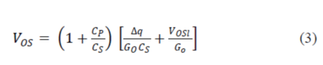 |
| Equations (2) and (3) show that, for similar preamplifiers, the residual offset obtainable using OOS can be smaller than that
for IOS. |
RESULT AND DISCUSSIONS |
| Performance analysis of preamplifier based dynamic comparator and its offset cancellations techniques are presented.
Power dissipation (PD), propagation delay, offset voltage and number of transistors has been considered as performance
metrics in the present analysis and investigations has been carried out at 130nm technology node [6]. All the circuits
schematic are constructed on S-edit and results are obtained using TSPICE 13.0 version. |
| Fig. 4 shows the comparison of average power consumption between preamplifier based dynamic comparator and its offset
optimization techniques i.e. output offset storage (OOS) technique and input offset storage (IOS) technique. For a good
circuit, power consumption should be low as possible. |
| Fig. 4 reveals that OOS technique has 13.57% and 22.76% less power consumption as compared to comparator before
applying the offset reduction techniques and IOS technique respectively. |
| Preamplifier based dynamic comparator and its offset optimization techniques have been compared for propagation delay in
Fig. 5. Delay of a circuit should be low as possible so that it can perform faster for a given signal. It has been concluded
from the Fig. 5 that delay of comparator before applying the offset reduction techniques is 163.32% and 68.26% less than
the OOS and IOS techniques respectively. |
| Low power consumption can only be achieved at the expense of decreased operating speed (high delay) [7]. To trade-off
between these two conflicting requirements it is useful to determine the power- delay product. Power-delay product is an
important performance criterion as it depicts the energy consumption of the circuit. Lower the value of PDP the more
effective is the circuit. |
| Fig. 6 shows the comparison of power-delay product between preamplifier based dynamic comparator and its offset
optimization techniques. Figure reveals that comparator before applying the offset reduction techniques consumes 56.06%
and 46.89% less energy when compared to OOS and IOS offset reduction techniques respectively. |
| Power-delay and number of transistors product describes the silicon area requirement of a circuit. Fig. 7 shows the
comparison of power-delay and number of transistors product between preamplifier based dynamic comparator and its
offset optimization techniques. It can be concluded from the figure that OOS technique consumes 20.88% and 127.59%
larger silicon area as compared to IOS technique and comparator before applying offset reduction technique respectively. |
| Fig. 8 shows the comparison of offset voltage between preamplifier based dynamic comparator and its offset voltage
optimization techniques. It is shown in the figure that a very large amount of offset voltage is reduced after applying offset
reduction techniques i.e. 99.56% by IOS technique and 99.62% by OOS technique. |
| Output offset storage technique can be used to achieve higher accuracy as the amount of offset voltage reduced in output
offset storage technique is 12.5% more than the input offset storage technique. |
Figures at a glance |
 |
 |
 |
 |
| Figure 1 |
Figure 2 |
Figure 3 |
Figure 4 |
 |
 |
 |
 |
| Figure 5 |
Figure 6 |
Figure 7 |
Figure 8 |
|
| |
References |
- Fayed and M. Ismail, “A High Speed, Low Voltage CMOS Offset Comparator”, in Analog Integrated Circuits and Signal Processing, vol. 36, pp. 267–
272, 2003.
- V. Katyal, R. L. Geiger, and D. Chen , “A New High Precision Low Offset Dynamic Comparator for High Resolution High Speed ADCs,” in Proc.
Asia Pacific Conf. Circuits Syst., Singapore, pp. 5–8, 2006.
- Nikoozadeh and B. Murmann, “An Analysis of Latch Comparator Offset Due to Load Capacitor Mismatch,” IEEE Transactions on Circuits and
Systems, vol. 53, no. 12, pp. 1398-1402, 2006.
- Ghazi, A. Rawi, “A New Offset Measurement and Cancellation Technique for Dynamic Latches.” IEEE International Symposium on Circuits and
Systems, vol. 5, pp. 149-152, 2002.
- R. Poujois B. Baylac, D. Barbier and J. Ittel, “Low-level MOS transistor amplifier using storage techniques,” IEEE International Conference on Solid-
State Circuits, ISSCC Dig. Tech. Papers, vol. 16, pp. 152-153, 1973.
- Berkeley Predictive Technology Model. Univ. Berkeley, Berkeley, CA. [online]. Available: http://wwwdevices.eecs.berkeley.edu/~ptm, 2006.
|