The impact of tiny chip has been far-reaching. Many of the electronic products of today, could not have been developed without it. Platform for these chips has been provided by Integrated Circuits (ICs). Since 40 decades ICs have been far revolutionized. Various advancement have been made in these ICs; but still there are some conditions imposed by the designers for proper working of IC. One of such condition exist in biasing of IC. While designing the IC from Bipolar Junction Transistor (BJT), designers introduce that the collector voltage of output BJT used in biased circuit should be greater than a defined minimum value. It implies that user should check every time that whether the circuit is following the specified condition or not. The proposed biasing circuit design in this paper has no such condition and the user will get much freedom.
Keywords |
| Current Mirror, Active Mode, Beta (β), Early Effect, Scale Current. |
I. INTRODUCTION |
| Since 1971 Integrated Circuits are the essence of Electronics Engineering. Transistors are frequently used active device
in these ICs. For operation of ICs proper biasing is essential. Nowadays several ‗active biasing‘ techniques have been
used to bias an IC (e.g. Simple Current Mirror, Current Mirror with Better β Insensitivity, Cascode Current Mirror,
Wilson Current Mirror, Widlar Current Source). Since last 20 decades improvements have been carried out in biasing
techniques. Laura Sanchez-Gonzalez, Gladys Ducodray-Acevedo presented a novel approach to improve the previous
current mirrors and increased the current input range with a lower error percentage and a high accuracy low voltage
dynamic self-biasing ([6]). Adjustable gain linear current gain mirrors are also presented. According to A. K. Gupta, J.
W. Haslett and F. N. Trofimenkoff, it can produce linear gain over several decades of signal current ([5]). Low voltage
application current source has been designed. The use of low voltage application current source improved the common
mode input range and the common mode rejection ratio of fully-balanced single ended differential amplifier by Fan
You, S.H.K. Embabi, J.F. Duque- Carrillo and Edgar Sanchez- Sinencio ([7]). But all of these biasing techniques
impose a condition on the output BJT, regarding its collector voltage i.e. output transistor should be operated in such a
manner that its collector voltage must be higher than a certain value. And during our operation we must keep this value
in mind. In the following section you will get familiar with a design that can bias an IC without imposing any condition
on the collector voltage of output transistor. The bias circuit is such that it will set its output transistor in the require
mode (active mode). |
II. CIRCUIT DESCRIPTION & SPECIFICATIONS |
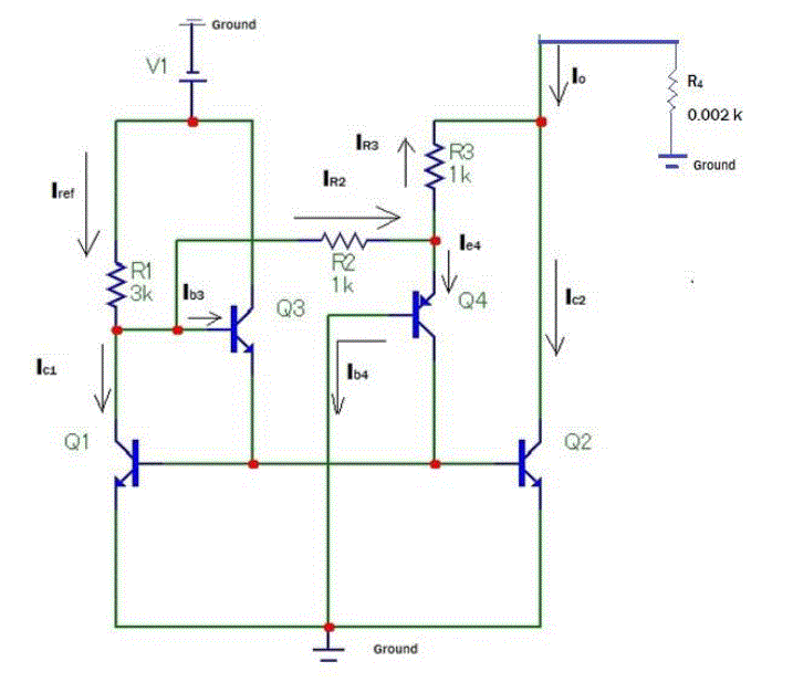
| Schematic of bias circuit is such that the base of transistor Q1 (npn) and Q2 (npn) are tied together as in Fig. 1. Their
emitter terminals are shorted with ground. Thus Q1 and Q2 are forming mirror. Q3 (npn) is introduced to reduce the
dependency of β on output current. Q4 (pnp) is to adjust Q3 in active mode. Base of Q4 is grounded and its emitter has
two branches, one going towards base of Q3 with resistance R2 and the other one towards collector of Q2 with resistance R3. Current flowing in all the branches are shown in Fig. 1. R1 is to generate desired reference current in whole circuit
with the help of supply voltage. |
| R1 = 3 kΩ |
| R2 = 1 kΩ |
| R3 = 1 kΩ |
| R4 = 0.002 kΩ (load resistance; adjustable according to our need) |
| Source voltage = 15 Volts |
III. CIRCUIT ANALYSIS |
 |
 |
 |
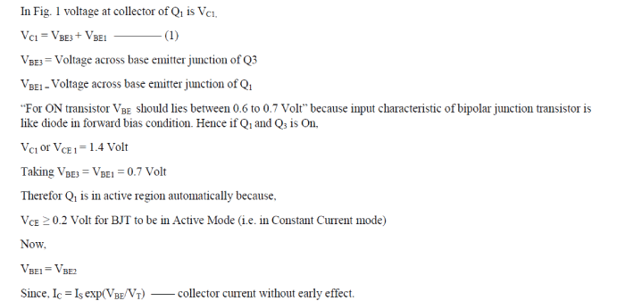
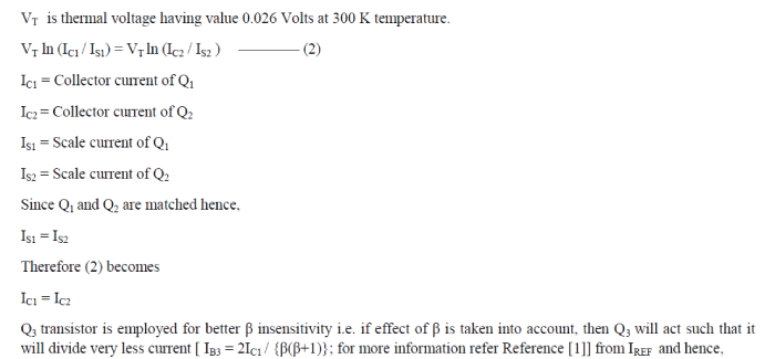
| And mostly all current which is flowing in R2 go towards emitter of Q4 because of R3 (i.e. R3 will draw less current).
Since Q4 is a pnp transistor hence it will also draw less current from R1 but not as much less as current flowing in R3.
Hence overall effect is that very less current will go towards R2 and that current is mostly divided at emitter of Q4. |
IV. COMPARISON FROM NORMAL CURRENT MIRROR WITH BETTER BETA INSENSITIVITY
Fig. 2 |
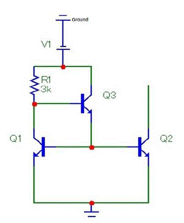
| In Fig.2, to act it as a perfect constant source VCE of Q2 should be greater than 0.2 Volts i.e. must be adjusted such that
at every level of analysis we must take care of this VCE value. |
| But in Fig.1 there is no need to take care VCE value of Q2 (or output transistor) because it automatically adjust itself in
active region (i.e. a perfect constant current source). |
V. EXPERIMENTAL RESULTS |
| When 15 Volts DC source is employed and R1, R2, R3 are taken as mentioned earlier. |
| VBE1 = VBE2 = 0.68 Volts (Q1 and Q2 are ON) |
| VBE3 = 1.38 – 0.68 = 0.7 Volts (Q3 is ON) |
| VCE1 = 1.38 Volts (Q1 is in active mode) |
| VCE2 = 1.1 Volts (Q2 is in active mode) |
| IR3 = 0.6 mA (very low) |
| IREF = 5.1 mA |
| IO = 5.0 mA |
| IR3 = Current flowing in R3 resistor |
VI. CONCLUSION |
| Though there are several Integrated Active Biasing circuits and also some of them have remarkable level of stability of
output current; but all active biased circuits suffer from a required value of collector voltage of its output transistor.
This illustrated design simplifies this flaw. Hence by using this design we can bias our IC chip more efficiently without
requiring adjustment of voltage at collector terminal. We will be more flexible in BiCMOS process using this design. |
Figures at a glance |
 |
 |
| Figure 1 |
Figure 2 |
|
| |
References |
- Adel S. Sedra and Kenneth C. Smith adapted by Arun N. Chandorkar, Microelectronic Circuits, 5th Ed., Oxford University Press.
- Aloke K. Dutta, Semiconductor Devices and Circuits,Oxford University Press.
- Donald A. Neamen, Semiconductor Physics and Devices, 3rd Ed., Tata McGraw Hill Education Private Limted.
- Paul R.Gray, Paul J. Hurst, Stephen H. Lewis, Robert G. Meyer, Analysis and Design of Analog Integrated Circuits, 4th Ed., John Wiley & Sons, INC.
- K. Gupta, J. W. Haslett and F. N. Trofimenkoff, ―BiCMOS Adjustable Linear Current Mirror”, IEEE Journal of Solid State Circuits, Vol. 32, No.1, January 1997.
- Laura Sanchez-Gonzalez, Gladys Ducodray-Acevedo, Member IEEE, ―High Accuracy Self-Biasing Cascode Current Mirror”.
- Fan You, S.H.K. Embabi, J.F. Duque- Carrillo and Edgar Sanchez- Sinencio, ―An Improved Current Source for Low Voltage Applications”, Custom Integrated Circuits Conference.
- Monfaredi K., ―A Novel Low Voltage Current Compensated High Performance Current Mirror”. Quality Electronic Design, 2010, 11th International Symposium.
- F. You, et al., ―An Improved Tail Current Source for Low Voltage Applications”, IEEE Journal os Solid State Circuits, Vol: 32, No. 8, August 1997, pp. 1173-1180
- Zhangming Zhu, Jianbin MO, Yintang Yang, ―A Low Voltage Bulk-driving PMOS Cascode Current Mirror”, Solid State and Integrated-Circuit Technology, ICSICT, 9th International Conference on IEEE, pp. 2008-2011, 2008
|