Analysis and design of a voltage doubler bridgeless buck converter is performed during the course of project and hardware implementation of a prototype was done during this period. Voltage doubler bridgeless buck converters can be used in switched mode power supplies as rectification as well as power factor correction circuit. Conventional switched mode power supplies contains a bridge rectifier followed by power factor correction circuit and second stage dc to dc converters for generating the required dc voltage.Bridgelesss voltage doubler circuit combines both the rectifier and power factor correction circuit to a single circuit, the output of which is double the voltage produced by a single buck converter [3] used as pfc circuit. This circuit consists of two buck converters connected in parallel in series out manner. The total output obtained is the sum of voltage across each capacitor of the buck converters which are operating during positive and negative half respectively. MOSFET is used as the switching device of the buck converter Usually pulse width modulation technique is used for switching operation and clamped current mode control is used for controlling the buck converter. In this paper ,a new control method called One Cycle Control is used for controlling the buck converter during both half of supply voltage. This method is a non linear control technique to control the duty ratio of the switch in real time such that in each half cycle the average value of the chopped waveform is made equal to the reference value. This method provides greater response and rejects input voltage perturbations.Simualation of the circuit employing One Cycle Control is done in MATLAB/SIMULINK .A prototype of voltage doubler buck converter generating a dc voltage of 12V operating at a switching frequency of 65kHz is developed. The gating signals are generated by microcontroller ATMEGA16 and the program is written in C language.PWM switching technique is used here as implementation of One Cycle Control required a better controller. The results obtained are also presented in this paper.
Keywords |
| Power Factor Correction, Bridgeless voltage Doubler, Buck Converter, One Cycle Control |
I. INTRODUCTION |
| Switch mode power supplies without power factor correction will introduce harmonic content to the input current
waveform which will ultimately results in a low power factor and hence lower efficiency. A bridge diode rectifier
followed by a power factor correction circuit which is either a buck or boost frontend is commonly used for all
switched mode power supplies. Boost converter as a PFC front-end exhibits 1-3% lower efficiency at 100-V line
compared to that at 230-V line. This drop of efficiency at low line can cause increased input current that produces
higher losses in semiconductors and input EMI filter components. Also it has relatively output voltage, typically in the
380-400-V range. This high voltage leads to switching losses of the primary switches of the downstream dc/dc output
stage and the size and efficiency of its isolation transformer. |
| At lower power levels the drawbacks of the universal-line boost PFC front-end may be overcome by implementing the
PFC front-end with the buck topology [7]. Since the output voltage of a buck converter is less, the dc/dc stage can be
implemented with lower-voltage-rated semiconductor devices and optimized loss and size of the transformer.
Conventional ac-dc converters has a diode bridge rectifier followed by power factor correction circuit .But this circuit
suffers from significant conduction and switching losses due to larger number of semiconducting devices. This problem
can be solved by using bridgeless converters to reduce the conduction losses and component count. A bridgeless buck
PFC rectifier[3] combines both rectification and power factor correction using a single circuit. This circuit also act as a
voltage doubler circuit whose output voltage is greater than a single buck converter. Usually the switching operation is controlled by pulse width modulation technique using clamped mode current control of a buck converter .This paper
explains a new control method called One Cycle Control [6] which is a non linear control technique and produce faster
response than the later one. |
II.BRIDGELESS BUCK PFC CONVERTER |
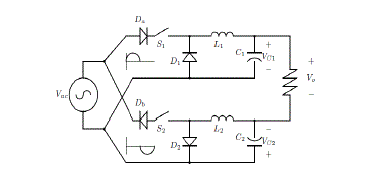
| Figure shows the PFC circuit formed by two buck dc/dc converters. Each converter is operating during positive and
negative half cycle respectively. This PFC rectifier employs two back-to-back connected buck converters that operate
in alternative halves of the line-voltage cycle. The buck converter operating during positive half-cycles of line voltage
Vac consists of a unidirectional switch comprising of diode Da in series with switch S1 freewheeling diode D1 , filter
inductor L1 and output capacitor C1. Similarly, the buck converter consisting of the unidirectional switch implemented
by diode Db in series with switch S2 , freewheeling diode D2 , filter inductor L2 , and output capacitor C2 operates only
during negative half-cycles of line voltage Vac . |
| The input current flows through only one diode during the conduction of a switch, i.e., either Da or Db . Efficiency is
further improved by eliminating input bridge diodes in which two diodes carry the input current. An additional
advantage of the proposed circuit is its inrush current control capability. Since the switches are located between the
input and the output capacitors, switches S1 and S2 can actively control the input inrush current during start-up.
Output voltage Vout of the PFC rectifier is the sum of the voltages across output capacitors C1 and C2 , is given by Vout
= 2DVin where d is the duty ratio |
III. PWM CONTROL OF SWITCHING CONVERTER |
| In pulse width modulation (PWM) control, the duty ratio is linearly modulated in a direction so as to reduces the error.
Any change in the input voltage must be sensed as an output voltage change and error produced in the output voltage is
used to change the duty ratio to keep the output voltage constant. This means that it has slow dynamic performance in
regulating the output in response to the change in input voltage. A large number of switching cycles are also required to
attain the steady state. |
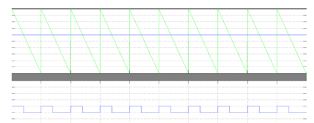
| In PWM control, the duty ratio pulses are produced by comparing control reference signal with a saw-tooth signal. As a
result the control reference is linearly modulated into the duty ratio signal. If the power supply voltage is changed, for
example by a large step up, the duty ratio control does not see the change instantaneously since the error signal must
change first. Therefore, the output voltage jumps up and the typical output voltage transient overshoot will be observed
at the output voltage. Then the error produced in the output voltage is amplified and compared with the saw tooth
signal to control the duty ratio pulses. |
| A large number of switching cycles is required before the steady-state is reached. The output is always influenced by
the input voltage perturbation. |
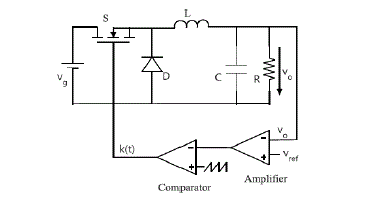
| The figure shows a typical buck converter using PWM technique .The voltage output Vo is compared with Vref to
generate an error signal and it is amplified.The error signal thus obtainedand saw tooth waveform is given as input to
the comparator where it is compared is compared to generate the PWM signal for the switch.Since the error generated
is used to vary the duty ratio to keep the voltage constant ,this method produce a slow response |
IV.ONE CYCLE CONTROL |
| One Cycle Control is a new nonlinear control technique implemented to control the duty ratio of the switch in real time
such that in each cycle the average value input waveform at the switch rectifier output diode is exactly equal to the
control reference. One-Cycle Control method [2] reject input voltage perturbations in only one switching cycle and
follow the control reference very quickly. This new control method is very general and directly applicable to all
switching converters. Switching converters are pulsed and nonlinear dynamic systems. This technique takes advantage
of the pulsed and nonlinear nature of switching converters and achieves instantaneous control of the average value of
the chopped voltage or current. This technique provides fast dynamic response and good input-perturbation rejection.
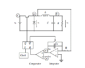
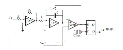
Figure shows a typical buck converter employing One Cycle control. The one-cycle controller is comprised of an
integrator with reset, a comparator, a flip-flop, a clock and an adder. The clock triggers the RS flip-flop to turn ON the
transistor with a constant frequency. When the switch is turned on by a fixed frequency clock pulse, voltage available
across the diode is being integrated. The output of the integrator is compared with the control reference in real time
using a comparator. |
| When the integrated value of the diode-voltage becomes equal to the control reference, the transistor is turned OFF and
the integration is immediately reset to zero to prepare for the next cycle. In each cycle, the diode-voltage waveform
may be different. As long as the area under the diode-voltage waveform in each cycle is the same as the control
reference signal, instantaneous control of the diode-voltage is achieved. Since the switched variable always follows the
control reference the output voltage is independent of all input voltage variations. |
| Figure shows a typical buck converter employing One Cycle control. The one-cycle controller is comprised of an
integrator with reset, a comparator, a flip-flop, a clock and an adder. The clock triggers the RS flip-flop to turn ON the
transistor with a constant frequency..When the switch is turned on by a fixed frequency clock pulse, voltage available
across the diode is being integrated. The output of the integrator is compared with the control reference in real time
using a comparator. |
| When the integrated value of the diode-voltage becomes equal to the control reference, the transistor is turned OFF and
the integration is immediately reset to zero to prepare for the next cycle. In each cycle, the diode-voltage waveform
may be different. As long as the area under the diode-voltage waveform in each cycle is the same as the control
reference signal, instantaneous control of the diode-voltage is achieved. |
| A.occ controller for bridgeless buck converter |
| Figue shows an OCC controller [2] for controlling a bridgeless buckconverter.Here Vo is the output voltage obtained
across the two capacitors C1and C2.The output obtained is amplified and is fed to an integrator with reset.At each
instant the integral value is being compared with a reference Vref .When integral value Vint reaches the control
reference,Vref comparator changes its state and turns the switch (transistor) off and the integrator is reset to zero at the
same time. Since the reset signal is a pulse with very short width, the reset time is very short, and the integration is
activated immediately after the resetting. |
| Thus, Vint = 1/RC ∫kVo(t)dt ,where k is the gain of the amplifier |
| The output of comparator is given to a flip flop to give signals to switches Q1 and Q2 |
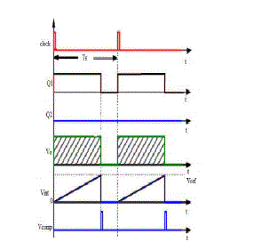
| The operation of an OCC controller is explained by means of the following waveforms. Here Ts is the time period of
one switching cycle. The operation is explained for positive half cycle during which switch Q1 is operating and Q2 is
off ,Vref is the reference voltage .The output voltage is obtained across the capacitor according the ON and OFF of the
switch. The integrator is also activated during the start of each switching cycle. When the integral value of Vo reaches
the Vref ,the comparator changes its state from low to high which is indicated by a short pulse as shown in the graph.
When this condition is reached the switch is turned off till the starting of the next switching cycle and this process
repeats for both positive and negative half. By increasing the switching frequency almost constant output voltage can
be obtained by this control method. This also eliminates any variation of the input supply voltage and provides a
dynamic performance |
V.SIMULINK MODEL OF BRIDGELESS BUCK CONVERTER AND OCC |
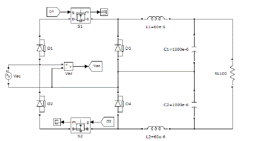
| The simulation of the proposed controller employed in Bridgeless Buck converter is done in MATLAB
SIMULINK.The simulink model of the bridgeless buck converter is shown below. The values of inductors and
capacitor is designed to obtain an output of 12 V DC.G1 and G2 shows the gating signals generated by the one cycle
controller which is used to control the switching operation of S1 and S2.The simulation is done at a switching
frequency of 65kHz.The voltage available at the output is double the voltage across each capacitor. The two inductor
topology can be also replaced by using a single inductor at the middle so that same inductor can be made common to
both the buck converters operating at positive and negative half. |
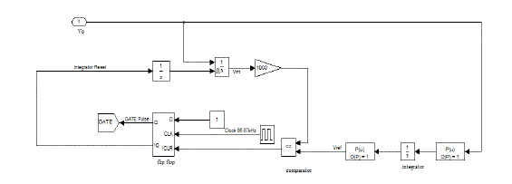
| The simulink model of OCC controller is shown below. The output voltage V0 is fed to the integrator .The output of the
integrator is compared with the reference in the comparator and the output of the comparator is used to set and resets
the D flip flop. The output of the flip flop is the required gating pulse for the switches |
| VI. SIMULATION RESULTS OF ONE CYCLE CONTROLLED BRIDGELESS BUCK CONVERTER |
| The simulation of the bridgeless buck converter operating at a switching frequency of 65kHz is done using
SIMULINK.The buck converter is generating an output voltage of 12V using One Cycle Control method. The gating
signals given to the switches during the positive and negative half cycle, input and the output waveforms obtained
during the simulation are shown below. When switching pulses are given to one of the switches the other switch will be
off. Thus it is important to identify whether the incoming waveform is from the positive half or from the negative half. |
VII. HARDWARE IMPLEMENTATION |
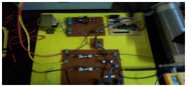
| The hardware setup of the circuit is designed and implemented .Here PWM switching technique is used for varying the
duty ratio of the switches and there by controlling the ON and OFF of the switches. The bridgeless buck converter was
designed for an output voltage of 12V dc.ATMEGA 16 is the controller used for generating the control signals. The
prototype of a typical converter is shown below.IRFP250N power MOSFET is used as the switching device whose
switching is controlled by the microcontroller ATMEGA 16L.TLP250 is used as power MOSFET gate driver.BYQ28E
is used as the diode rectifier. Two capacitors of 1000μF is used for each set of buck converter which is operating during
the positive and negative half cycle. Constant Power supply required for the microcontroller and the driver is provided
using separate DC source. Supply required for the operation of other semiconductor devices is being supplied by the
power supply unit being implemented within the circuit. |
VIII.EXPERIMENTAL RESULTS |
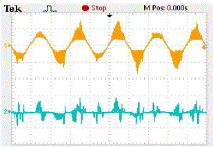
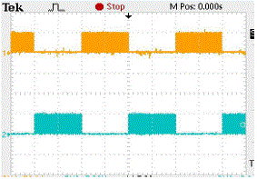
| The results obtained during the hardware implementation are presented below. The input voltage and current
waveforms, gating signals and the output obtained are shown. |
VIII.CONCLUSION |
| The bridgeless voltage doubler buck converter configuration has been studied. This circuit generates the output voltage
which is double than a conventional buck converter since it is having two buck converters operating in a complete
cycle. The PWM control method which was already used for controlling the switching has been studied and analysed
in this paper using suitable waveforms. A new control method called One Cycle Control has been implemented to the
bridgeless buck converter in order to get dynamic response and to eliminate the input voltage perturbations. Since the
output voltage always follows the switched variable the output remains constant at the reference value .This method
also eliminates the use of various control loops thus reducing the complexity of the conventional cicuit.The simulation
of bridgeless buck voltage doubler circuit using One Cycle Control was done in Matlab simulink and the waveforms
obtained at the time of simulation is presented here. The hardware implementation for the prototype is made for 12V dc
and PWM technique is used as the switching technique. Microcontroller ATMEGA 16 is used as the controller. As a
future work the hardware circuit should be implemented using one cycle control. |
ACKNOWLEDGMENT |
| First and foremost, I would like to thank God Almighty for his assuring presence and blessings as it was only through
his grace I was able to complete my project successfully. |
| I extend my deep sense of gratitude and hearty thanks to Prof. K Radhakrishnan (HOD, Electrical and Electronics
Engineering Department) for his inspiration and support to do the project internally. I would like to thank my internal
guide Prof. Leena Thomas, Professor, EEE Department, MACE for her valuable guidance, support and timely advice given to me during the course of the project. I also render my sincere thanks to all the professors of electrical and
electronics department of MACE for their valuable suggestions given to me during the completion of my thesis work
Last but not the least I sincerely thank my parents and husband for all their support and encouragement and for the
sacrifices they have made, that helped me to complete the project successfully. |
Figures at a glance |
 |
 |
 |
 |
| Figure 1 |
Figure 2 |
Figure 3 |
Figure 4 |
 |
 |
 |
 |
 |
| Figure 6 |
Figure 7 |
Figure 8 |
Figure 9 |
Figure 10 |
 |
 |
 |
 |
 |
| Figure 11 |
Figure 12 |
Figure 13 |
Figure 14 |
Figure 15 |
|
| |
References |
- Sen.P.C.," Modern Power Electronics ", Wheeler publishing Co, First Edition, New Delhi
- Dongsheng Yang, Min Yang, and XinboRuan, “One Cycle Control for a Double –Input DC/DC Converter” ,” IEEE Trans. Power Electron., vol. 27, no. 11, Nov. 2012
- YungtaekJang,Milan M Jovanovic “Bridgeless High Power Factor Buck Converter,” IEEE Trans. Power Electron., vol. 26, no. 2, pp .02– 611, Feb. 2011.
- L. Huber, L. Gang, and M. M. Jovanovi´c, “Design-OrienteD analysis and performance evaluation of buck PFC front- end,” IEEE Trans. Power Electron., vol. 25, no. 1, pp. 85–94, Jan. 2010
- [4 ]G. Spiazzi, “Analysis of buck converters used as power factor preregulators,” in Proc. IEEE Power Electron. Spec.Conf. (PESC)Rec., Jun. 1997
- Keyue. M. Smedley and C. Slobodan, “One-cycle control of switching converters,” IEEE Transactions on Power Electronics, vol. 10, no. 6, Nov.1995
- H. Endo, T. Yamashita, and T. Sugiura, “A high-power-factor buck converter, in Proc. IEEE Power Electron. Spec Conf. (PESC) Rec., Jun. 1992, pp. 1071–1076
- www.ijert.org
- www.google.com.au/patents/US7304457
- www.wikepedia.com
- www.ijetae.com
|