Keywords
|
| System-On-Chip (SoC), Memory test, Spare elements, Syndrome Storing-Based Detection (SSD), Must- Repair Analyzer. |
I.INTRODUCTION
|
| Embedded memories tend to have a greater impact on the overall chip area, where SoC occupy more than 60% thereby concentrating on the yield.[2]. Built-in redundancy analysis (BIRA) is a technique used for repair analysis, this method involves achieving high yield of memory by use of additional good cells. [6]. The previous technique describes analysis of memory element one at a time therefore in order to achieve high speed and optimum repair rate, an analyzer involving evaluation of nodes in parallel is an efficient BIRA with an optimum repair rate. [5]. In-order to improve the yield of the SoC spare memory is utilized. Utilization of spare memory column for the replacement of faulty memory element is provided. [1]. |
| Incorporating both spare rows and columns improves the efficiency to the great extent so, additional row and column memory is incorporated into the memory array in the wafer. [7]. Basically faults are of two types. They are soft and hard fault. Soft fault occurs due to transmission of data or congestion of data in the transmission line and these faults are temporary faults. Hard faults are also called as permanent faults, they may occur due to environmental defects like temperature variation, manufacturing defects, etc… .In all these method replacement of memory takes place without the consideration of type of fault. With the intention to overcome the demerits that are obtained in the previous techniques such as unwanted replacement of memory in the case of soft fault, non optimum exploitation of spare memory ,soft fault memory element’s address which is stored in Must Repair Analyzer (MRA) leading to increase in the memory entries are all overcome by the proposed method. |
II. REPAIR ANALYSIS
|
| The block diagram consists of must-repair analysis and final analysis. Must-repair rows and columns are identified by the must- repair analysis, and the final analysis involves determining repair solution. The must-repair analysis and the test are performed concurrently; after the test is completed the final analysis is done. If a particular row or column is recognized as must-repair, the solution consists of row or column address partly. Thus the solution record is filled with the row and column address by MRA. Fig 1 shows the block diagram of BISR design. A shift register whose input bit is a linear function of its previous state is a linear-feedback shift register, which involves in test pattern generation The most commonly used linear function of single bits is XOR. An LFSR is for the most often a shift register whose input bit is driven by the exclusive-or of some bits of the overall shift register value. |
| The initial value of the LFSR is called the seed, and for the reason that the operation of the register is deterministic, the flow of values created by the register is completely determined by its current (or previous) state. Similarly, in due course the register must enter a repeating cycle due to the reason it has a finite number of possible states. However, an LFSR with a suitable feedback function can generate a series of bits which appears random and which has a very long cycle. |
| Applications of LFSRs include generating pseudo-random-numbers, fast digital counters, pseudo-noise sequences and whitening sequences. Mutual hardware and software implementations of LFSRs are common.The schematic of Bit- Swapping LFSR is shown in fig 2. The mathematics of a cyclic redundancy check, used to endow with a quick check aligned with transmission errors, are intimately related to those of an LFSR. |
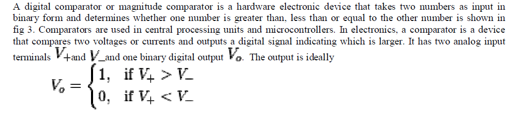 |
| A comparator consists of specialized high-gain differential amplifier. They are commonly used in devices that measure and digitize analog signals, such as analog-to-digital converters, as well as relaxation oscillators. When a comparator performs the function of telling if an input voltage is above or below a given threshold, it is effectively performing a 1- bit quantization. This function is used in almost all analog to digital converters (such as flash, pipeline, successive approximation, delta-sigma modulation, folding, interpolating, dual-slope and others) in combination with other devices to achieve a multi-bit quantization. |
| Syndrome decoding is a common technique for decoding linear block codes. The syndrome is calculated by matrix multiplication S= uHT where u is a received code word vector of length n (u= c+ e, where c is a transmitted code word and e is an error vector, both of length n), HT is the transpose of (n- k) * n the parity-check matrix, and s is a syndrome vector of length n- k . The syndrome gives the minimum weight error vector index, so the error vector e can easily be determined. The correction is done by c= u+ e, eliminating the error from the received data word.The basic idea behind Syndrome storing based detection(SSD) is that the error syndrome of an error control code contains information about the errors of a received code word. |
| If the syndromes of a number of consecutive received code words are the same, then it can be concluded that there is a permanent error in the link (limitations described momentarily). The error location can be extracted from the syndrome using the normal decoding procedure. An important design decision for the SSD method is to determine how many syndromes to consider before deciding that an error is permanent. We refer to this number of cycles as the observation period top . |
| If an intermittent error is misdiagnosed as a permanent error, a spare wire is consumed. In SSD, there is no method for recovering spare wires once they have been assigned, so the error observation period can result in wasted wire resources if set too short. On the other hand, too long an observation period may result in a large number of cycles before the error is detected or may even leave errors undetected. This is because the detection of stuck-at faults is data dependent; in order to be detected, the error must occur in all data words during the observation period. For example, a stuck-at-1 fault can only be detected if all the data bits passing through that wire over top cycles are 0. The upper limit for the number of cycles before the permanent error should be detected can be derived from the transient bit error rate (BER). Since a permanent error in a link may prohibit the detection and correction of a transient error, the number of cycles to detect a permanent fault should be much smaller than the mean time between transient errors. |
| The structure of the SSD circuit is given in fig 4. It contains a register to store the syndrome, a comparator between the input and the last syndrome, and a counter for counting the number of identical but nonzero syndromes. The counter is reset during a reconfiguration procedure, which is achieved using the busy signal. By changing the width of the counter, top can be easily changed. |
III. RESULTS AND DISCUSSIONS
|
| The fig 5 describes the simulation result of memory write operation involving generation of 8-bit test pattern using linear feedback shift register, and the generated test pattern is written in to memory array of [0-15] among the array of [257] each module of 8-bit wide and the rest of the array is filled with default value. |
| Simulation result of fault injection, memory read operation is shown in fig 6. It shows the operation of injecting the fault into the memory array since there is no chance of fault in the soft memory module. Fault is injected into the memory array of [4,9,14] and after fault injection the data is read from memory array and proceeded with the next operation of fault location. |
| The type of error is determined before repair analysis by sending consecutive inputs to the obtained faulty address, fig 7. The identified faulty address is repaired by replacing the faulty memory module data with the required data (11110101) as shown in the simulation result of fault repair operation, fig 8. Thus the fault repair with an optimum repair rate has been obtained. |
IV. CONCLUSION AND FUTURE ENHANCEMENT
|
| An On-Chip infrastructure for repair analysis with the optimal repair rate have been proposed. A complete reconfigurable system utilizing spare wires to replace erroneous wires and enabling reconfiguration with the single test has been presented. Error detection involves Syndrome Storing- Based Error Detection method, which is based on evaluation of consecutive code syndromes at the receiver. |
| The bit-line sense amplifier for on-chip flash memory compares cell current with reference current to identify data that are programmed. The S/A for 0 (erased) cell data consumes a large sink current, which is greater than off-current for 1 (programmed) cell data. The future enhancement may involve a built-in write/read path based on binary inversion methods to reduce the sensing current of S/A. An original binary code is programmed into flash memory with an inverted binary code based on the proposed bit inversion techniques. The de-inversion hardware, which is implemented with small logic gates to restore original binary data, only consumes logic current instead of analog sink current in the S/A. |
Figures at a glance
|
 |
 |
 |
 |
 |
| Figure 1 |
Figure 2 |
Figure 3 |
Figure 4 |
Figure 5 |
 |
 |
 |
 |
| Figure 6 |
Figure 7 |
Figure 8 |
Figure 9 |
|
| |
References
|
- A. Ferris and G. Work, “Memory circuit capable of replacing a faulty column with a spare column,” U.S. Patent 5 163 023,1992.
- S. Hamdioui, G. Gaydadjiev, and A. van de Goor,“The state- of- art and future trends in testing embedded memories, ” in Proc. Records Int.Workshop Memory Technol., Design, Test.,2004.
- C.-T. Huang, C.-F. Wu, J.-F. Li, and C.-W. Wu,“Built-in redundancy analysis for memory yield improvement,” IEEE Trans. Reliab., vol. 52, no. 4, pp. 386–399, 2003.
- Jaeyong Chung, Member, IEEE, Joonsung Park, Member, IEEE, and Jacob Abraham, Fellow, IEEE,“A Built- In Repair Analyzer With Optimal Repair Rate for Word-Oriented Memories” IEEE Trans, Very Large Scale Integration(VLSI) Systems, Vol. 21, No. 2, 2013.
- W. Jeong, J. Lee, T. Han, K. Lee, and S. Kang,“An advanced BIRA for memories with an optimal repair rate and fast analysis speed by using a branch analyzer,” IEEE Trans. Comput.-Aided Design Integr. Circuits Syst.,2010.
- W. Jeong, I. Kang, K. Jin, and S. Kang,“A fast built-in redundancy analysis for memories with optimal repair rate using a line-based search tree,” IEEE Trans. Very Large Scale Integr. (VLSI) Syst.,2009.
- S.-Y. Kuo and W. Fuchs,“Efficient spare allocation for reconfigurable arrays ,” IEEE Design Test Comput., vol. 4, no. 1,pp. 24–31,1987.
- N. MacDonald,“Memory array of integrated circuits capable of replacing faulty cells with a spare,” U.S. Patent 5 406 565,1995.
- TeijoLehtonen, Student Member, IEEE, David Wolpert, Student Member, IEEE, PasiLiljeberg, Member, IEEE, JuhaPlosila, Member, IEEE, and Paul Ampadu, Member, IEEE,”Self-Adaptive System for Addressing Permanent Errors in On-Chip Interconnects”,2010.
- Y. Zorian and S. Shoukourian,“Embedded-memory test and repair: Infrastructure IP for SOC yield,” IEEE Design Test Comput., vol. 20, no. 3, pp. 58–66,2003.
- R. Rajsuman, “Design and test of large embedded memories: An overview,” IEEE Design Test Comput., vol. 18, no. 3, pp. 16–23, May 2001.
|