International Journal of Advanced Research in Electrical, Electronics and Instrumentation Engineering
ISSN ONLINE(2278-8875) PRINT (2320-3765)
ISSN ONLINE(2278-8875) PRINT (2320-3765)
J. Salai Thillai Thilagam1, Dr. P. K. Jawahar2
|
| Related article at Pubmed, Scholar Google |
Visit for more related articles at International Journal of Advanced Research in Electrical, Electronics and Instrumentation Engineering
A simulation of sixteen (hexadeci) faced microstrip patch antenna design using slit on the edge is discussed here. This antenna is fed using probe feed model. It is simulated using IE3D electromagnetic simulator. The simulated results of the antenna achieve the radiation parameters such as scattering parameter (S-parameter), radiation pattern and voltage standing wave ratio (VSWR). In S-parameter, the S11 parameter value is reached < -10 dB for the resonant frequencies 0.9 GHz, 0.87 GHz to 0.90 GHz and VSWR value is obtained < 2 for that same frequencies. The proposed antennas will be useful for 900 MHz band in wireless communication applications.
Keywords |
| Microstrip Antenna, Patch Antennas, Probe Feed, Wireless Communication |
I. INTRODUCTION |
| An antenna converts an electromagnetic signal to an electrical signal at a receiver or electrical signal to an electromagnetic signal at a transmitter. It is also the interface between transmitter lines and space. The importance of wireless communication systems increase efforts devoted to the design and implementation of novel microstrip structures from miniaturized electronic circuits to the antenna arrays [19]. |
| One major application is design of microstrip antenna arrays which are attractive candidates for adaptive systems in the present and future communication systems. Their main advantages are light weight, low cost, planar or conformal layout, and ability of integration with electronic or signal processing circuitry [23, 24]. |
| A microstrip patch antenna consists of a radiating patch on one side of a dielectric substrate which has a ground plane on the other side. The patch is generally made of conducting material such as copper or gold and can take any possible shape. The radiating patch and the feed lines are usually photo etched on the dielectric substrate [25]. In order to simplify analysis and performance prediction, the patch is generally square, rectangular, circular, triangular, and elliptical or some other common shape [4]. |
| Microstrip patch antennas radiate primarily because of the fringing fields between the patch edge and the ground plane. For good antenna performance, a thick dielectric substrate having a low dielectric constant is desirable since this provides better efficiency, larger bandwidth and better radiation [26]. However, such a configuration leads to a larger antenna size. In order to design a compact microstrip patch antenna, a compromise must be reached between its dimensions and performance to get efficient antenna [7]. Cutting slits on the edge of the excited patch surface make fractal design for the microstrip antenna [9]. |
| In this paper, the hexadeci faced patch antenna with slit on edge is introduced to simulate them and get good radiation properties. The remainder of the paper is organized as follows. Section II provides the literature survey of the proposed hexadeci faced patch antenna [5]. Section III provides the analysis and design of the proposed hexadeci faced patch antenna [6]. Section IV gives experimental results for the conventional patch antenna with probe feed and proposed meandered line patch. The results demonstrate that an enhancement of the gain significantly the matching of the patch antenna. Finally, concluding remarks are given in Section V. |
II. LITERATURE SURVEY |
| In this section, the microstrip antenna literature survey is discussed. Tae-Hyun Kim, Dong-Chul Park (2005) presents a compact dual-band antenna with double L-slits for wireless local area network (WLAN) applications in IEEE 802.11a/b/g. The proposed antenna effectively covers both 2.4/5-GHz bands with three resonances that are caused by the double L-slits. The proposed antenna has compact size of 15 mm×9 mm×7 mm, which is only half size of the antenna using double U-slots [11]. |
| A.Al-Zoubi et al (2009) presented a broadband center-fed circular patch-ring antenna with a monopole like radiation pattern [17]. R. Kumar et al (2010) designed a CPW–Fed Ultra wideband Fractal Antenna and Backscattering Reduction [18]. Garima et al (2011) proposed antenna with improved bandwidth in hexadeci faced patch antenna [21]. |
| The circular microstrip antenna offers a number of radiation pattern options not readily implemented using a rectangular patch. The fundamental mode of the circular microstrip patch antenna is the TM11. This mode produces a radiation pattern that is very similar to the lowest order mode of a rectangular microstrip antenna. The next higher order mode is the TM21, which can be driven to produce circularly polarized radiation with a monopole-type pattern [8, 10]. This is followed in frequency by the TM02 mode, which radiates a monopole pattern with linear polarization. In the late 1970s, liquid crystals were used to experimentally map the electric field of the driven modes surrounding a circular microstrip antenna and optimize them [1]. |
| In Figure 1, the geometry of a circular microstrip antenna is defined. The circular metallic patch has a radius „aâÃâ¬ÃŸ and a driving point located at „râÃâ¬ÃŸ at an angle „φâÃâ¬ÃŸ measured from the x- axis. As with the rectangular microstrip antenna, the radiating patch is spaced at a distance „hâÃâ¬ÃŸ from a ground plane. A substrate of εr separates the patch and the ground plane. |
| An analysis of the circular microstrip antenna, which is very useful for engineering purposes, has been undertaken by Derneryd and is utilized here[2]. The electric field under the circular microstrip antenna is described by: |
| EZ = E0 Jn (kr)cos(nφ) (1) |
| The magnetic field components are described as Hr and Hφ in eq.(2) and (3) |
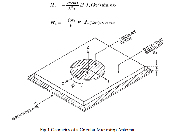 |
| Where „kâÃâ¬ÃŸ is the propagation constant of the dielectric substrate. Jn is the Bessel function of the first kind of order n. J´n is the derivative of the Bessel function with respect to its argument,ω is the angular frequency (=2πf). The TM21 mode has the next highest frequency of operation (after TM11). This particular mode is useful in creating a monopole radiation pattern that has circular polarization, as described by Huang [3]. It is possible to drive a patch in the TM21 mode with a single feed which will produce circular polarization [10]. |
| VSWR is the ratio between the maximum voltage and the minimum voltage along the transmission line. The VSWR and reflection coefficient is given by the equation shown eq. (4), (5). |
| VSWR = (1+ Γ)/ (1- Γ) (4) |
| Where Γ is the reflection coefficient |
| Γ = (ZL-Z0)/ (ZL+Z0) (5) |
| The VSWR indicate that how closely or efficiently an antennaâÃâ¬ÃŸs terminal input impedance is matched to the characteristic impedance of the transmission line. The larger the number of VSWR provides, the greater the mismatch between the antenna and the transmission line. |
| An antennaâÃâ¬ÃŸs radiation pattern is the characteristics that most affect system coverage and performance. All antennas do not radiate more total energy than is delivered to their input connector. Antenna radiation pattern are typically presented in the form of a polar plot for a 360° angular pattern in one of two sweep planes and it is presented on a relative power dB scale [13]-[16]. |
| Relative permittivity of the substrate is an important parameter to consider. It is because relative permittivity will enhances the fringing fields that account for radiation. This type of antenna is characterized by its length L, width w, and thickness. |
| The other radiation pattern properties of significance are the antennaâÃâ¬ÃŸs side lobes, back lobes and front to back ratio (f/b). In practice, it is impossible to eliminate antenna side lobes and back lobes completely. |
| Antenna side and back lobes affect antenna and system performance in several ways. First, energy delivered to or received by side and back lobes is from a direction other than the intended region of coverage and is therefore wasted. |
| At a transmitter, energy delivered to side and back lobes maybe directed towards other receive systems causing interference. Then at a receiver, energy from other transmit sites may be received through the side and back lobes causing interference within the system. |
| Main lobe is the radiation lobe containing the direction of the maximum radiation. For side lobe, it is a radiation lobe in any direction other than the intended lob direction. It is usually adjacent to the main lobe and occupies the hemisphere in the direction of the main beam. A radiation lobe in which axis is at 180° with respect to the main beam. It usually refers to a small lobe that occupies the hemisphere in a direction opposite to a main lobe are the definition for back lobe. |
| Looking at the current (magnetic field) and voltage (electrical field) for a single circular patch, the current is maximum at the centre and minimum near the left and right edges, while the electrical field is zero at the centre and maximum near the left and minimum near the right edges, as in Fig.2 |
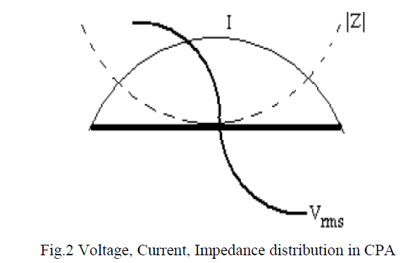 |
| From the magnitude of the current and voltage, we can conclude that the impedance is minimum at the middle of the patch and maximum (around 200 Ω, but depend on the Q of the leaky cavity) near the edges. Hence, there is a point where the impedance is 50Ω along the “resonant length” at x-axis of the element. I, Z expressions are given in eq. (6) and (7) below. |
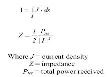 |
| Mathematically speaking, impedance can be computed if the current distribution is known [15]. |
III. ANALYSIS AND DESIGN |
| In this section, the microstrip antenna analysis, design methodology is discussed. The fist design step is to select a suitable dielectric substrate material. The major electrical properties considered here are relative dielectric constant εr and loss tangent tan (δ). Generally it is best to select a substrate with the lowest possible dielectric constant consistent with the space available for the antenna. Substrate thickness should be chosen as large as possible to maximize |
| bandwidth and efficiency, but not so large as to risk surface-wave excitation [22]. The analysis is carried out by calculating the radius „aâÃâ¬ÃŸ, from the given data such as dielectric constant, height, resonant frequency, etc. |
| Theoretically the radius of circular patch antenna is calculated from the expression as in eq.(8) given below by |
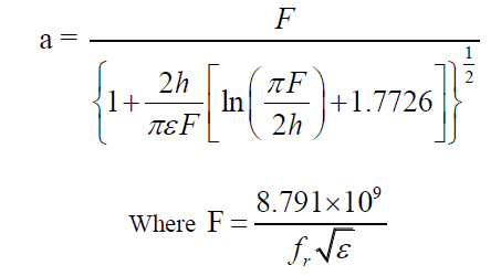 |
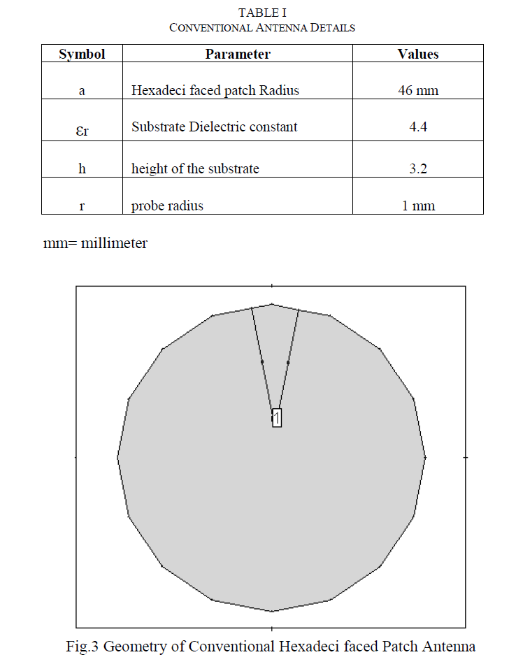
| fr is resonant frequency. The circular microstrip patch antenna geometry [28] is shown in Fig. 1. We proposed a hexadeci faced microstrip antenna with a radius of 46 mm on a dielectric substrate that is 3.2 mm thick and has a relative dielectric constant of εr = 4.4 and tan δ = 0.0009 to illustrate the properties of the TM11 mode. Conventional antenna details are shown in Table I. |
 |
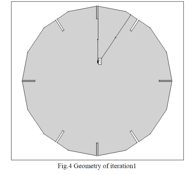
| A. Hexadeci faced microstrip patch antenna iteration1 |
| This antenna designed for the resonant frequency 0.9 GHz is shown in Fig. 4. The patch antenna is hexadeci faced with a radius of a = 46 mm with 8 rectangular slits of each 8mm x 1mm on the edge surface and is printed on a substrate with a relative permittivity of εr = 4.4 and a thickness of h = 3.2 mm. The patch is fed by a probe with a radius of 1 mm placed at feed point (1.185, 11.8) of the patch. The feed location was optimized to give good impedance matching. The size of the substrate is 200 mm X 200 mm. The antenna resonates at 0.89 GHz. |
 |
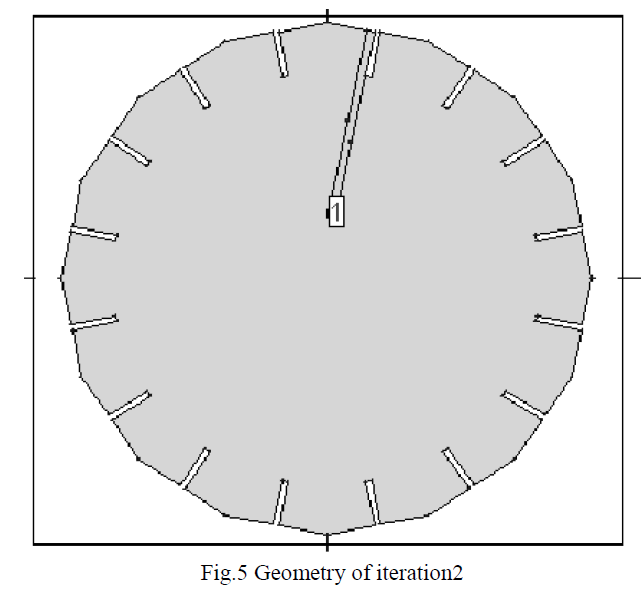
| B. Hexadeci faced microstrip patch antenna iteration2 |
| The patch antenna is hexadeci faced with a radius of a = 46 mm with 16 rectangular slits of each 8mm x 1mm on the edge surface and is printed on a substrate with a relative permittivity of εr = 4.4 and a thickness of h = 3.2 mm. The patch is fed by a probe with a radius of 1 mm placed at feed point (1.185, 11.8) of the patch. The feed location was optimized to give good impedance matching. The size of the substrate is 200 mm X 200 mm. This iteration2 is shown in fig.5 |
 |
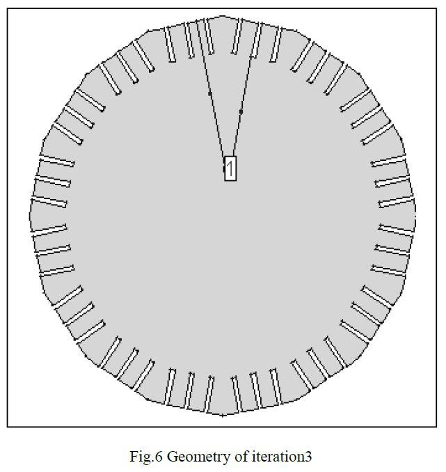
| C. Hexadeci faced microstrip patch antenna iteration3 |
| This patch antenna is hexadeci faced with a radius of a = 46 mm with 48 rectangular slits of each 8mm x 1mm on the edge surface and is printed on a substrate with a relative permittivity of εr = 4.4 and a thickness of h = 3.2 mm. The patch is fed by a probe with a radius of 1 mm placed at feed point (1.185, 11.8) of the patch. The feed location was optimized to give good impedance matching. The size of the substrate is 200 mm X 200 mm. this iteration3 is shown in fig.6 |
 |
IV. RESULT AND DISCUSSION |
| The proposed hexadeci faced patch antennas using probe feed are designed. They are simulated in IE3D electromagnetic simulator software [27]. The results are given in following figures 7-8 and it is compared in the table II. |
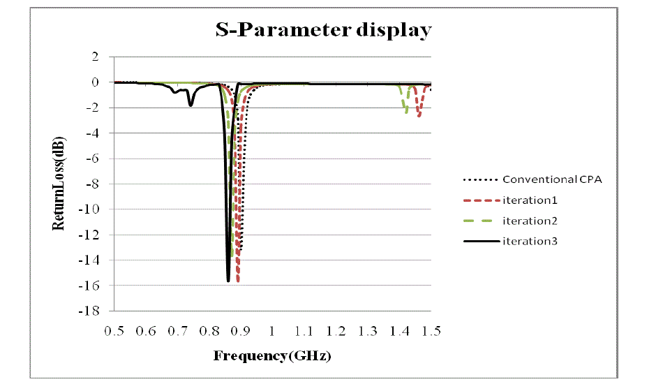 Figure 7: Return Loss versus Frequency of conventional, iteration1-3 antennas |
| From the iteration1 graph it is understood that the resonant occurs at the frequency 0.89 GHz for the return loss - 15.67 dB. From the S-parameter display of iteration2 graph it is understood that the resonant occurs at the frequency 0.87 GHz for the return loss -13.64 dB. The simulated VSWR value is 1.5 for the same frequency and it is recorded in the table II. The S-parameter display of conventional, iteration1-3 is shown in Fig.7. From this graph it is understood that the resonant occurs at the frequency around 0.9 GHz for the return loss -15.63 dB. |
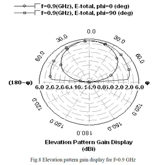
| From this figure 8, it is noted that how the radiation pattern distribution takes place in the patch. The antenna impedance parameter for the proposed hexadeci faced patch antenna is close to 50 ohms for the resonant frequencies. During the simulation the total field gain, directivity, Radiation Efficiency, antenna efficiency of antennas is noted and shown in Table II. The dielectric constant, εr primarily affects the bandwidth and radiation efficiency of the antenna. |
 |
| The antenna with lower permittivity will give a wider impedance bandwidth and reduce the surface wave excitation. The comparison of antennas [12] is furnished in the table II. |
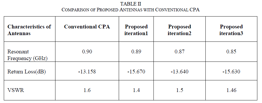 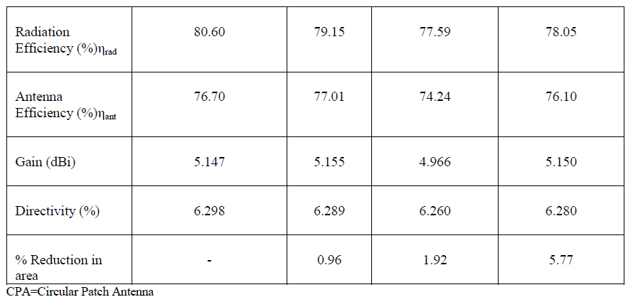 |
| From these comparison results, it is understood that iteration of antenna makes the reduction in frequency with the reduction of area. |
V. CONCLUSION |
| In this paper, we have analyzed a hexadeci faced microstrip antenna with slits on the edge. It is simulated in IE3D software. Simulations have been carried out to investigate the antennaâÃâ¬ÃŸs performance and characteristics. The simulation result shows good agreement with theoretical values. The antennas proposed can be built and measured to compare the real results with those obtained from the simulations as a future work. Possible applications of this antenna include RFID, UHF applications. |
ACKNOWLEDGMENT |
| The author is thankful to the Dean and Head of the Department, Electronics and Communication Engineering, B. S. Abdur Rahman University, Chennai for providing research facility and valuable suggestions for this work. |
References |
|