Keywords
|
| Common Mode Voltage, Sinusoidal Pulse width modulation, Phase Disposition Phase Opposition Disposed, Alternatively in Opposition disposition |
I. INTRODUCTION
|
| Energy saving has never been more important than it is today where the demand is increasing and the production is not catching up to the demand. The general consumption of electricity is in motor pump where the electrical energy gets converted in mechanical energy by motors. So there is a need to find out ways to improve power utilization and decrease the losses.The Invertor connected with these devices have switching devices which are connected in series to raise the blocking capacity in conventional two-level MV inverters. The switching devices are connected in series to raise the blocking capacity in conventional two-level MV inverters. The simultaneous switching of series connected fast devices generates voltage with a high dv=dt at the output terminal of the inverter. The combination of a short rise time of the inverter output voltage and a long cable are potentially hazardous for the motor insulation and the cable itself. The phenomenon, which is worsened with a shorter rise time, appears on motors as a leakage current. In motor drive applications, this may lead to electromagnetic interference noise that causes a nuisance trip of the inverter drive, problems with the protection scheme of the supply transformer and interference with other electronic equipment in the vicinity [1]. In addition, a conventional two-level inverter based drive faces problems with the CMV. The CMV is responsible for the shaft voltage and the premature failure of the bearings [2]. It is very important to reduce CMV itself or to limit this voltage to within certain bounds. Some approaches have been presented to cope with the CMV issue include four leg inverters, passive filters, passive elements with active circuitry and dual bridge inverters [3]–[6]. |
| A multilevel inverter can reduce as well as eliminate the CMV. Multilevel inverters have a high number of switching states so that the output voltage is stepped in smaller increments. This allows mitigation of the harmonics at low switching frequencies thereby reducing switching losses. Further, the leakage current is reduced because of the lower dv=dt. The H-bridge multilevel inverter presented in literature has been implemented successfully in industrial applications for high power drives. However, the drawback is that these inverters need a large number of dc sources or isolation transformers on the ac side. The diode clamped multilevel structure is more suitable for high and medium voltage drives which are directly connected to the utility power system (direct to drive topology). This topology requires only one ac power supply (with a front end active converter and an inverter at the drive end) therefore; itis very attractive for industrial adjustable speed drives (ASD). The CMV reduction technique is well discussed in many papers using a higher level cascaded H Bridge multilevel inverter and a three-level diode (neutral) clamped inverter.The application of a five-level diode clamped inverter to reduce common mode voltage using POD-PWM has not been reported in literature. |
II. SPWM TECHNIQUES
|
| Recently, several methods to implement SVM for multilevel converters have been presented. These techniques have been successfully used to reduce as well as cancel the CMV. In [7], a five-level inverter is used to eliminate CMV but the levels of the phase voltages of the star connected load are reduced from five to three and the magnitude of the line voltage transition increases. The same source also reported that the trade off between the magnitude of the CMV and the switching states gives rise to lower order harmonics in the phase voltage. In this paper CMV reduction is proposed using the Phase Disposition(PD) Phase Opposition Disposed(POD), Alternatively in Opposition disposition(APOD) SPWM technique. |
III. COMMON MODE VOLTAGE
|
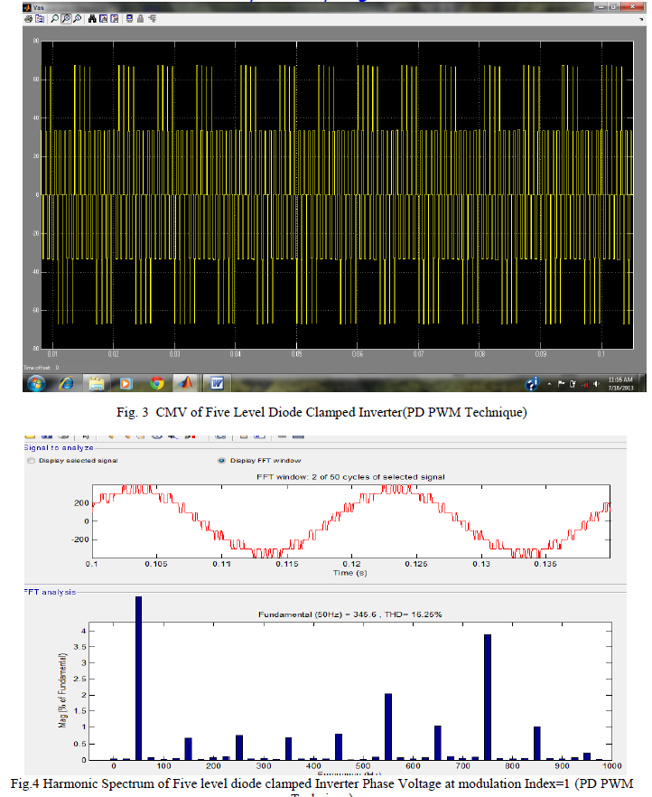
| CMV is defined as the voltage at the star point of the load and the system ground. The magnitude of the CMV depends on grounding system. In this paper, CMV is defined with respect to the dc midpoint (Vcom in Fig. 2) because this definition of CMV consists of the well defined edges that are responsible for common mode current. |
 |
| `Since the VSI cannot provide purely sinusoidal voltages and has discrete output voltages synthesized from the fixed dc bus voltage Vdc, the CMV is always different from zero and may take the values of _Vdc=6 or _Vdc=2, depending on the inverter switch states selected. During the switch state changes, the CMV changes by _Vdc=3, regardless of the changing states. The change in CMV from Vdc=2 to -Vdc=6 constitutes step of Vdc=3. When the level changes from - Vdc=6 to Vdc=6, the change is again Vdc=3. The use of three-level technology with existing device ratings is not sufficient, therefore, internal series connection is necessary [10]. This configuration gives the advantages of a low dv=dt, a low harmonics magnitude and a high quality output at a low switching frequency. The drawback of the additional requirement of a clamping diodes can be justified by eliminating the equalization circuit, the lower magnitude of the harmonics at a low switching frequency, less THD at a low switching frequency, low switching losses, a low dv=dt, a reduced or zero CMV and a smaller size sine filter, dv=dt filter and/or CMV filter. This topology is also suitable for retrofitting. |
IV. MODULATION TECHNIQUES
|
| A fundamental issue in the control of a multilevel converter is to determine the switching angles (times) so that the converter produces the required fundamental voltage and does not generate specific lower order dominant harmonics. The selective harmonic elimination PWM (SHEPWM) technique for multilevel inverters has the theoretical potential to achieve the highest output power quality at a low switching frequency in comparison to other modulation methods. With the same number of stages as fundamental switching, SHEPWM provides more degree of freedom to eliminate the more specific lower order harmonics without increasing the amount of hardware. The main challenge associated with the SHEPWM technique is to obtain the analytical solution of the system of nonlinear transcendental equations that contains a trigonometric turn providing multiple sets of solutions. |
| Carrier based modulation techniques control each phase leg of an inverter separately and allow the line to line voltage to be developed implicitly. In contrast, SVM identifies each switching state of a multilevel inverter as a point in complex space. Then a reference phasor rotating in the plane at the fundamental frequency is sampled within each switching period, and the nearest three inverter switching states are selected with duty cycles calculated to achieve the same volt second average as the sampled reference phasor. This directly controls the inverter line to line voltages, and only implicitly develops the phase leg voltages. Conventional two-level hysteresis current control operates by comparing a current error (i.e., the difference between the measured and the demanded phase currents) against a fixed hysteresis band. When the error falls below the lower hysteresis limit, the inverter phase leg output is switched to high, and when the error rises above the upper hysteresis limit, the inverter output switches to low. Unlike conventional twolevel inverters, multilevel inverters use numerous dc levels for the synthesis of their output voltage waveforms. The hysteresis current control of multilevel inverters therefore requires additional logic to select an appropriate voltage level at any time instant so as to confine the current error to within the hysteresis band. |
| The SPWM technique does not require computation therefore, this technique is easy to implement on-line in a digital controller. |
V SIMULATION AND EXPERIMENTAL RESULTS
|
 |
 |
 |
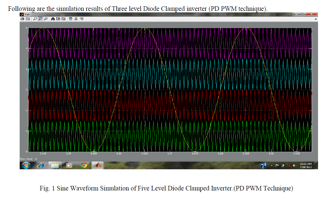
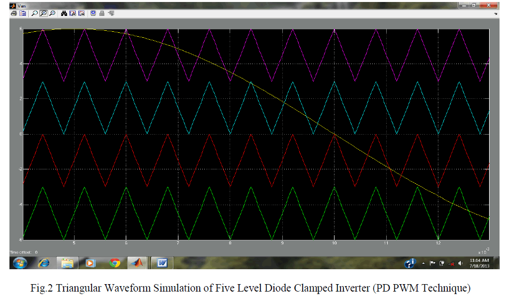
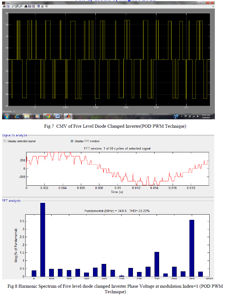
| A. Phase Opposition Disposition (POD): |
| Five level Diode Clamped inverter (POD PWM technique) is modeled based on the theoretical concepts explained in chapter 3.1 & 4.2.1 (b). The Carrier frequency 2500 Hz is taken for simulation. Following are the simulation results of Three level Diode Clamped inverter (POD PWM technique). |
 |
 |
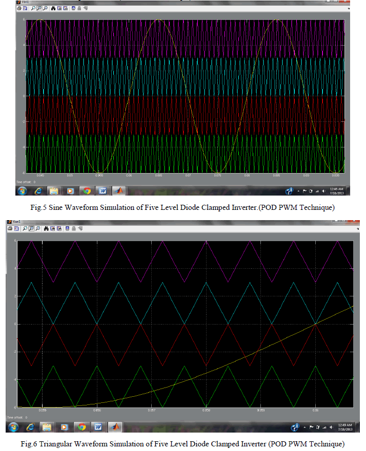
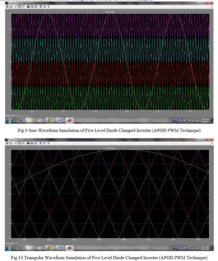
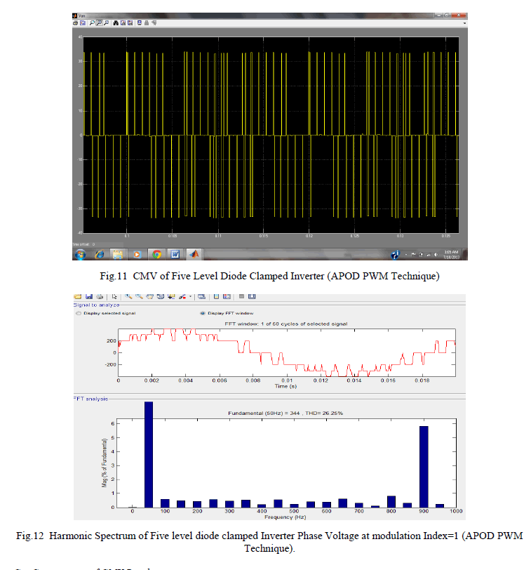
| B. Alternate Phase Opposition Disposition (APOD): |
| Five level Diode Clamped inverter (APOD PWM technique) is modeled based on the theoretical concepts explained in chapter 3.1 & 4.2.1 (c). The Carrier frequency 2500 Hz is taken for simulation. Following are the simulation results of Three level Diode Clamped inverter (APOD PWM technique). |
 |
 |
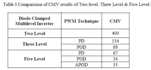
| C. Comparision of CMV Results: |
| The Comparision between the CMV results of Two Level, Three Level & five Level Diode Clamped Inverter Induction Motor drive is explained as reference to Table 1. |
 |
| This chapter presented the performance of multilevel inverter induction motor drives. We can observe that the quality of voltage and current waveforms increases with voltage level. The notches in the current and voltage waveforms reduce with increase in voltage level. Thus comparing the results it is observed that CMV has been predominantly reduced and drives performance improved. |
V. CONCLUSION
|
| In this paper we have provided a brief summary of multilevel inverter circuit topologies (2- level, 3-level and 5-level) and their analysis with respect to induction motor drives. Each MLI has its own mixture of advantages and disadvantages and for any one particular application, one topology will be more appropriate than the others. Often, topologies are chosen based on what has gone before, even if that topology may not be the best choice for the application. The advantages of the body of research and familiarity within the engineering community may outweigh other technical disadvantages. Multilevel converters can achieve an effective increase in overall switch frequency through the cancellation of the lowest order switch frequency terms. Among the multilevel converter topologies, the CMC is the most promising alternative for industry application. |
| There are many modulation techniques for multi level inverters. But carrier based modulation technique is easy and efficient. The PWM output spectra were calculated from basic operation simulated using MATLAB. The simulation results for two level, three-level and five-level diode clamped inverters are presented . The Comparision between the CMV results of Two Level, Three Level & five Level Diode Clamped Inverter Induction Motor drive is explained in Table 1 and from this analysis we are concluded that Five Level Diode clamped (APOD PWM Technique) inverter induction motor drive is best suited for the industrial application. |
References
|
- Yoshihiro Murai, Takehiko Kubota, and YoshiriroKawase, “Leakage current reduction for a high-frequency carrier inverter feeding aninduction motor,” IEEE Trans. Ind. Appl., Vol. 28. No. 4, pp. 858-863, Jul./Aug. 1992.
- Doyle F. Busse, Jay M. Erdman, Russel J. Kerkman, David W. Schlegel, and Gray L. Skibinski, “Bearing current and their relationship toPWM drives,” IEEE Trans. Indl. Electron., Vol. 12, No. 2, pp. 243-252, Mar. 1997.
- Hirofumi Akagi, and Shunsuke Tamura, “A Passive EMI filter for eliminating both bearing current and ground leakage current from aninverter-driven motor,” IEEE Trans. Power Electron., Vol. 21, No. 5, pp. 982-989, Sep. 2006.
- Chenggang Mei, Juan Carlos Balda, and William P. Waite, “Cancellation of common-mode voltages for induction motor drives usingactive method,” IEEE Trans. Energy Conversion, Vol. 21, No. 2, pp. 380-386, Jun. 2006.
- Haoran Zhang, Annette Von Jouanne, and Shaoan Dai, “A reducedswitched dual bridge inverter topology for the mitigation of bearingcurrent, EMI, and dc voltage variation”, IEEE Trans. Ind. Appl., vol. 37. No. 5, pp 1365-1372, Sep./Oct. 2001.
- GopalMondal, K. Gopakumar, P. N. Tekwani, and Emil Levi, “A reduced-switch-count five-level inverter with common-mode voltageelimination for an open-end winding induction motor drive,” IEEE Trans. on Indl. Electron., Vol. 54, No. 4, pp. 2344-2351, Aug. 2007.
- M. M. Renge, and H. M. Suryawanshi, “Five-level diode clamped inverter to eliminate common mode voltage and reduce dv=dtinmedium voltage rating induction motor drives,” IEEE Trans Power Electron., Vol.23, No. 4, pp. 1598-1607, Jul. 2008.
|