Key Terms
|
| Boost converters, dc–dc converters, high voltage gain, voltage multiplier cells (VMCs). |
INTRODUCTION
|
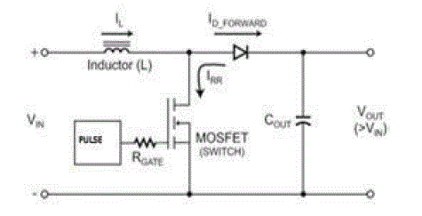
| A DC-to-DC converter is a device that accepts a DC input voltage and produces a DC output voltage. Typically the output produced is at a different voltage level than the input. In addition, DC-to-DC converters are used to provide noise isolation, power bus regulation, etc. Boost converter is used when a higher output voltage than input is required. |
| While the transistor is ON VIN =Vin, and the OFF state the inductor current flows through the diode giving Vx =Vo. For this analysis it is assumed that t h e i n d u c t o r c u r r e n t a l w a y s r e m a i n s f l o w i n g (Continuous conduction).The average v o l t a g e a c r o s s t h e i n d u c t o r must be zero for the average current to remain in steady state |
 (1) (1) |
| this can be rearranged as |
 (2) (2) |
| And for a loss less circuit the power balance ensures |
 (3) (3) |
| Since the duty ratio "D" is between 0 and 1 the output voltage must always be higher than the input voltage in magnitude. The negative sign indicates a reversal of sense of the output voltage. |
DC-DC CONVERTER WITH VMC
|
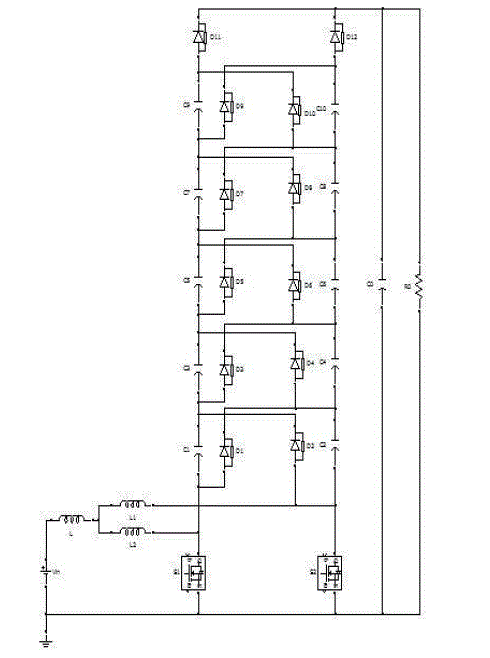
| The proposed dc-dc converter has 3ssc and 5 VMC cascaded to produce the high voltage gain. The topology used in the proposed method is that the two boost converters are coupled. So that the current is equally shared between two switches and the voltage doubler characteristics is also achieved. And also interleaving effectively reduces the input output current ripples. Hence the size of the energy storage inductor is reduced. |
PROPOSED TOPOLOGIES
|
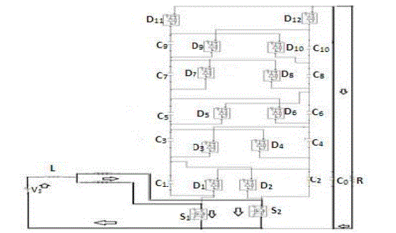
| The main circuit diagram of proposed dc-dc converter with 3 state switching cells and five voltage multiplier cells is shows in fig.2. |
| In this circuit diagram the switches S1 and S2 are MOSFETs. These Metal oxide semiconductor field effect transistors with reduced on resistance can be used to minimize conduction loss. This proposed topology for voltage step-up applications based on the use of multiplier cells constituted by diodes and capacitors. The converter is able to operate in overlapping mode (when a duty cycle D is higher than 0.5) and nonoverlapping mode (duty cycle is lower than 0.5). |
OPERATING PRINCIPLE
|
| Mode 1 |
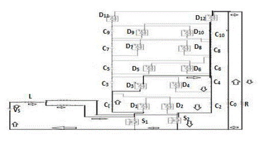
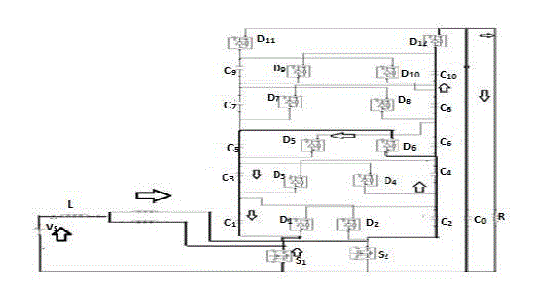
| Switches S1 and S2 are turned ON, while all Diodes are reverse biased. Energy is stored in Inductor L and there is no energy transfer to the load. The output capacitor provides energy to the load. |
| Mode 2 |
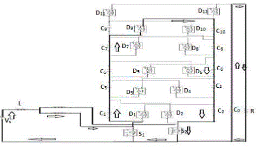
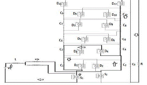
| Switch S1 is turned OFF, while S2 is still turned ON and diodeD9 is forward biased. There is no energy transfer to the load as well. Inductor L stores energy, capacitors C1, C3, C5 and C7 are discharged, and capacitors C2, C4, C6, C8 and C10 are charged. |
| Mode 3 |
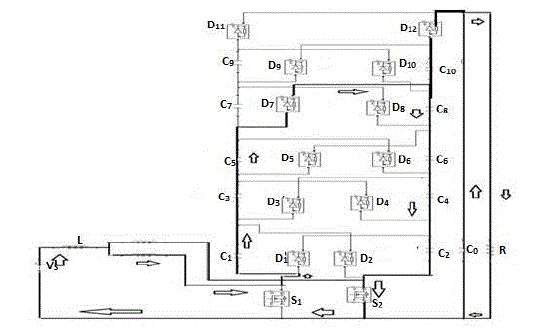
| Switch S1 is turned OFF, while S2 is still turned ON and diode D7 is forward biased, while all the remaining ones are reverse biased. Energy is transferred to the output stage through D12 .Inductor L stores energy, capacitors C1, C3 and C5 are discharged, and capacitors C2, C4, C6, C8 and C10 are charged. |
| Mode 4 |
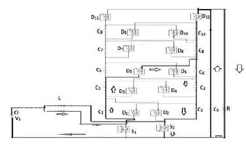
| Switch S1 is turned OFF, while S2 is still turned ON and diodeD5 is forward biased, while all the remaining ones are reverse biased. Energy is transferred to the output stage through D12. Inductor L stores energy, capacitors C1 and C3 are discharged, and capacitors C2, C4, C6, C8, and C10 are charged. |
| Mode 5 |
| Switch S1 is turned OFF, while S2 is still turned ON and diodeD3 is forward biased while all the r e mai ni ng o n e s a r e r ever se b iased . Energy is transferred to the output stage through D12. Inductor L stores energy, capacitor C1 is discharged, and capacitors C2, C4, and C6, C8, C10 are charged |
| Mode 6 |
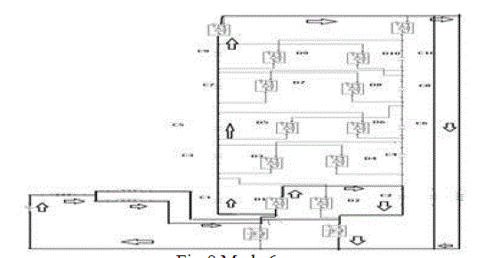
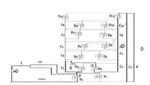
| Switch S2 remains turned ON, diode D3 is reverse biased, and diode D1 is forward biased while all the remaining ones are reverse biased. Energy is transferred to the load through D11 . The inductor is discharged, and so are capacitors C1 , C3 , and C5, C7, C9 while C2 is charged. |
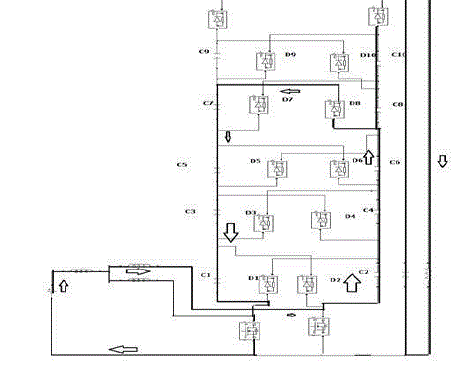
| Switches S1 turned ON, DiodeD8 is forward biased, w h i l e a l l t h e r e m a i n i n g o n e s a r e r e v e r s e biased. Energy is transferred to the output stage through D12. The inductor stores energy and capacitors C1, C3, C5, and C7 are charged. Capacitors C2 are discharged, and so are C4, C6, C8, and C10. |
| Mode 9 |
| Switches S1turned ON, Diode D6 is forward biased, while all the remaining ones are reverse |
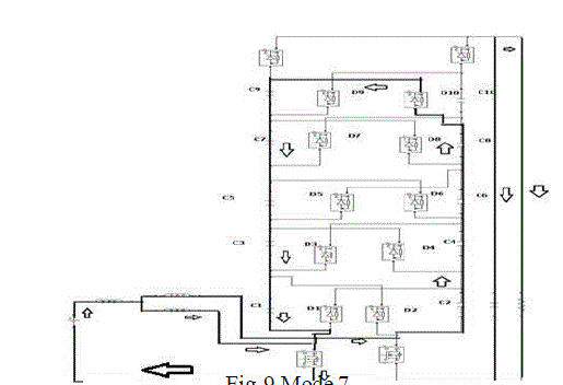
| Mode 7 |
| Switch S2 is turned OFF and switch S1 is still turned ON. Diode D10 is forward biased while all the remaining ones are reverse biased. The inductor is charged by the input source, although capacitors C2, C4, C6, and C8 are discharged and the capacitors C1, C3, C5, C7, and C9 are charged. |
| Biased. Energy is transferred to the output stage through D12. The inductor stores energy, and capacitors C1and C3, C5, are charged. Capacitors C2 are discharged, and so are C4 and C6, C8, C10. |
| Mode 10 |
| Switches S1turned ON, Diode D4 is forward biased, w h i l e a l l t h e r e m a i n i n g o n e s a r e r e v e r s e biased. Energy is transferred to the output stage through D12. The inductor stores energy and capacitors C1and C3 are charged. Capacitor C2 is discharged, and so are C4 and C6, C8, C10. |
| Energy is transferred to the output stage through D12. The inductor stores energy and capacitors C1 is charged. Capacitors C2 are discharged, and so are C4 and C6, C8, C10. |
DESIGN CALCULATION
|
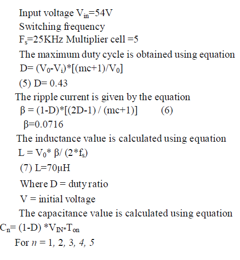 |
| Mode 11 |
| Switches S1turned ON, Diode D2 is forward biased, w h i l e a l l t h e r e m a i n i n g o n e s a r e r e v e r s e biased. |
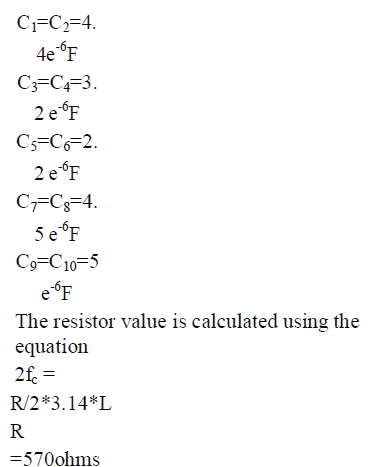 |
SIMULATION RESULTS
|
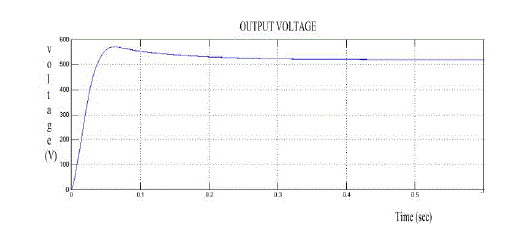
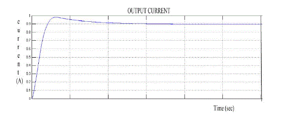
| The voltage increases by cascading several voltage multiplier cells constituted by diodes and capacitors. The voltage stress across the elements is reduced due to clamping performed by the output capacitor. The topology used in this method is that the two boost converters are coupled so that the current is equally shared between the switches and the voltage doubler characteristics is also achieved. The proposed structure with five multiplier cells has been designed and implemented with MATLABSIMULINK software. The input voltage of 54V is given and output voltage of 540V is obtained which is approximately ten times the input voltage |
CONCLUSION
|
| This project has proposed non isolated high voltage gain DC-DC converters. A novel high step up boost converter with voltage multiplier cell is presented. The voltage multiplier cell allows voltage to step up ten times its input while maintaining a moderate duty ratio. It is also expected that converters based on the 3SSC and 5VMC may be competitive solutions for high current and high voltage step up applications. Furthermore, only part of the energy from the input source flows through the active switches, while the remaining part is directly transferred to the load without being processed by these switches, i.e., this energy is delivered to the load through passive components, such as the diodes and the transformer windings The topology is adequate for several applications such as photovoltaic systems, fuel cell systems, UPS and Renewable energy. |
| |
Figures at a glance
|
 |
 |
 |
 |
 |
| Figure 1 |
Figure 2 |
Figure 3 |
Figure 4 |
Figure 5 |
| |
 |
 |
 |
 |
 |
| Figure 6 |
Figure 7 |
Figure 8 |
Figure 9 |
Figure 10 |
| |
 |
 |
 |
 |
 |
| Figure 11 |
Figure 12 |
Figure 13 |
Figure 14 |
Figure 15 |
|
| |
References
|
- S.V.Araujo, R.P.Torrico-Bascope, G.V. Torrico-Bascope, and L. Menezes, “Step- up converter with high voltage gain employing three state switching cell and voltage multiplier,” in Proc. Power Electron. Spec.2008, pp. 2271–2277.
- R.A. Da Camara, C.M.T. Cruz, and R.P. Torrico-Bascope, “Boost based on three- state switching cell for UPS applications,” in Proc. Brazilian Power Electron. 2009, pp. 313–318.
- K.C. Tseng and T.J. Liang, “Novel high- efficiency step-up converter,” IEE Proc. – Electr. Power Appl., vol. 151, no. 2, pp. 182–190, Mar. 2004.
- M. Prudente, L. L. Pfitscher, G.Emmendoerfer, E . F. Romaneli, a n d R . Gules, “Voltage multiplier cells applied to non-isolated converters,” IEEE Trans. Power Electron. vol. 23, no. 2, pp. 871–887, Mar. 2008.
- Y.R. Novaes, A. Rufer, and I. Barbi, “A new quadratic, threelevel, dc/dc converter suitable for fuel cell applications,” in Proc. Power Convers.Conf., Nagoya, Japan, 2007, pp. 601–607.
- K.C.Tseng and T. J.Liang, “Novel high- efficiency step-up converter,” IEEE Proc. – Electr. Power Appl., vol. 151, no. 2, pp.182–190, Mar. 2004
|