Keywords
|
| Polarization diversity, Printed dipole antenna, High frequency pin diode, HFSS simulation software. |
I. INTRODUCTION
|
| TodayâÃâ¬ÃŸs requirement for the effective wireless communication is that the received signal should be without any fading and degradation in the signal components. Multipath propagation effect degrades usually the wireless system performances. Signal fading due to the multi-path propagation can be reduced using antenna diversity techniques, most commonly introduced by two antenna functions at the mobile terminal. Antenna Diversity in one of the several methods that have been studied to mitigate this phenomenon. This technique can overcome the multipath fading improving the overall performance of communication system. This will leads to design such an antenna which will provide the effective communication in complicated environment. |
| Due to the presence of large buildings or towers or any other obstacle in the signal path, wireless signal may get distorted from its original path. So, the characteristics of the signal such as polarization, SNR ratio get changed. The polarization diversity antenna will provide the best solution to this problem. The antenna will be designed at 2.4GHz centre frequency which is suitable for wireless LAN applications. The implementation of antenna diversity can increase the channel capacity and reduce the multi-path interference. The condition for diversity antennas is that they should be of the same type and gain[10]. |
| Antenna diversity involves the use of multiple antennas to receive multiple instances of the same signal. This allows the system to be more robust against the many factors that degrade signal reliability. A single antenna may not be able to receive a signal for several reasons. The transmission of one polarization is depolarized by the propagation medium resulting in two orthogonal polarizations with uncorrelated fading variations. This diversity mechanism is very practical because of the very small size of antennas that can be used. It is also the mechanism that is mostly combined with space diversity. Two polarizations, vertical and horizontal, from two antennas can carry two signals on one radio frequency over wireless links. |
| Two orthogonal printed dipole antennas are designed fed by using a via hole balun. In particular, the microstrip line at the top layer feeds the dipole arms, and the integrated balun helps to cancel the current flowing on the outside part of the outer conductor at the coaxial line that is connected to the SMA connector[9]. |
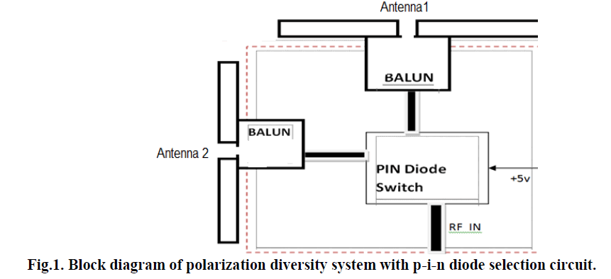
| A p-i-n diode selection ckt. is used to switch between two particular antennas to select the desired polarization, so that receiving the signal with minimum fading is possible. A PIN diode, designed for high frequency operation is usually fabricated to have low capacitance because the reactance of the diode in the OFF condition must be large compared to the line impedance.The basic block diagram of the system is shown below in figure (1). |
 |
II. ANTENNA DESIGN
|
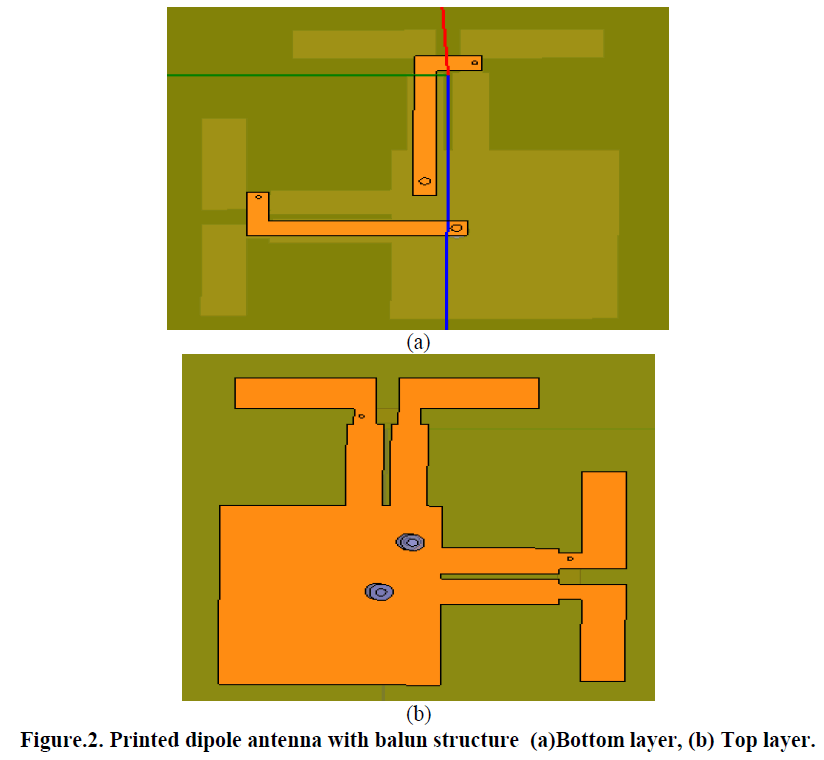
| The simulation part of printed dipole antenna is done by using HFSS simulator. A FR4 substrate with thickness of 1.6 mm and dielectric constant of 4.4 is selected for the design of whole circuit. The use of via hole balun helps to show the broadband nature of the dipole. The via-hole connects the microstrip line on the top layer to the right dipole arm on the bottom layer. This dipole arm will now have the same phase as the microstrip line. The dipole arm length and the microstrip feed line are approximately quarter-wavelength at the resonant frequency [1]. |
| Figure (2). below shows the top and bottom layer of printed dipole antenna. The via hole balun structure is used to feed the current to the dipole structure on the another side. A microstrip via-hole balun acts as an unbalance-to-balance transformer from the feed coaxial line to the two printed dipole strips. The lengths of the dipole-arm strip and the microstrip balun are all approximately a quarter wavelength [5]. |
 |
III. PIN DIODE SELECTION CRITERION
|
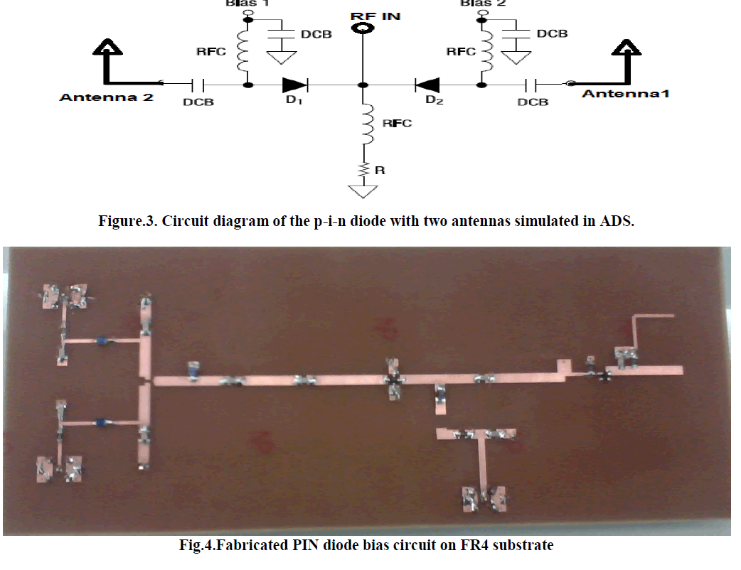
| A SMP-1321 series PIN diode from Skyworks solutions is used for polarization switching between the vertical and horizontal components of the linearly polarized wave[11]. The performance characteristics of the PIN diode depend mainly on the chip geometry and the processed semiconductor material in the intrinsic or I - region, of the finished diode. When the diode is forward biased, holes and electrons are injected into the I-region. This charge does not recombine instantaneously, but has a finite lifetime ( t ) in the I-region. If the PIN diode is reverse biased , there is no stored charge in the I-region and the device behaves like a Capacitance (CT) shunted by a parallel resistance (RP).The terminals of the balun are connected to pin diode ckt. A bias voltage of 3V is fed through dc line. The bias ckt. includes resistors, RF-choke inductors, and dc-block capacitors. |
| A unique feature of the PIN diode is its ability to control large amounts of RF power with much lower levels of DC. When the control current is switched on and off, or in discrete steps, the device can be used for switching. In addition, the PlNâÃâ¬ÃŸs small size, weight, high switching speed, and minimized parasitic elements make it ideally suited for use in miniature, broadband RF signal control components. In the design of a strip line or microstrip SPDT PIN diode switch, bandwidth and physical construction are often important considerations. When a switch is not performing satisfactorily, the fault is often not due to the PIN diode but to other circuit limitations such as circuit loss, bias circuit interaction, or lead length problems. |
| The equivalent R-L-C circuit models of a p-i-n diode containing packaged parasitic effects can be extracted from the measured S-parameters as shown in figure (3). The p-i-n diodes are with self-protect resistors of forward-biased current, RF choke inductors, and dc block capacitors to isolate the dc bias from the RF signal. The dc block capacitors should have very low impedance at the RF frequency, while the RF choke inductors should have very high RF impedance. A quarter wavelength meander line can be on the PCB substrate to replace the RF choke inductors. Since the maximum forward-bias current of the p-i-n diode[5] (HSMP-1321) is If =10 mA (with a forward voltage Vf =0.85V), a self-protect resistor R=3Ω should be added for the forward-bias 5 V. A dc block capacitors with C=0.25pF to have a very low impedance at the RF frequency is chosen. Figure (3) & (4) below shows the simulated and fabricated structure of two printed dipoles with p-i-n diodes and its bias circuit in ADS component library respectively. |
 |
IV. FABRICATED MODEL
|
| When two antennas are positioned near each other, and one or both of them are excited, some energy tends to end up at the other antenna. This interchange of energy is called mutual coupling and is a mechanism of great significance for antenna system performance. It depends on radiation characteristics of the antennas, relative separation between them and their orientation. |
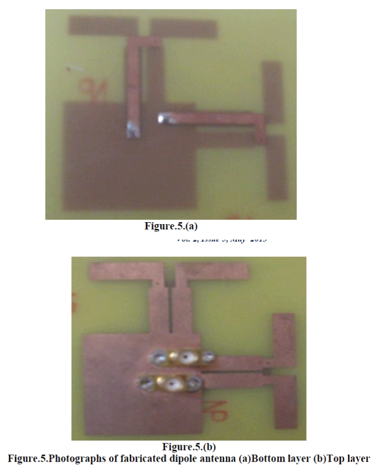
| The simulated model parameters of the printed dipole antenna in HFSS are used to fabricate the same model on FR4 substrate as shown in figure (5).The substrate thickness is 1.6mm with dielectric constant 4.4. The conductor thickness of the copper on patch side is 50μn. The table (1) below gives the structural parameters used for the antenna that will helps to achive good results. |
 |
 |
V. RESULTS AND DISCUSSIONS
|
| By using the transient data obtained from simulation, the surface current distribution on the metal plates can then be obtained directly from the tangential magnetic fields at centre frequency. The principle of simulation of field pattern is that one antenna at a time is excited while the other is terminated with a 50 ohm load. For S-parameter measurements the antenna system (both antennas) was simulated as a whole. |
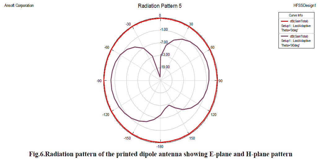
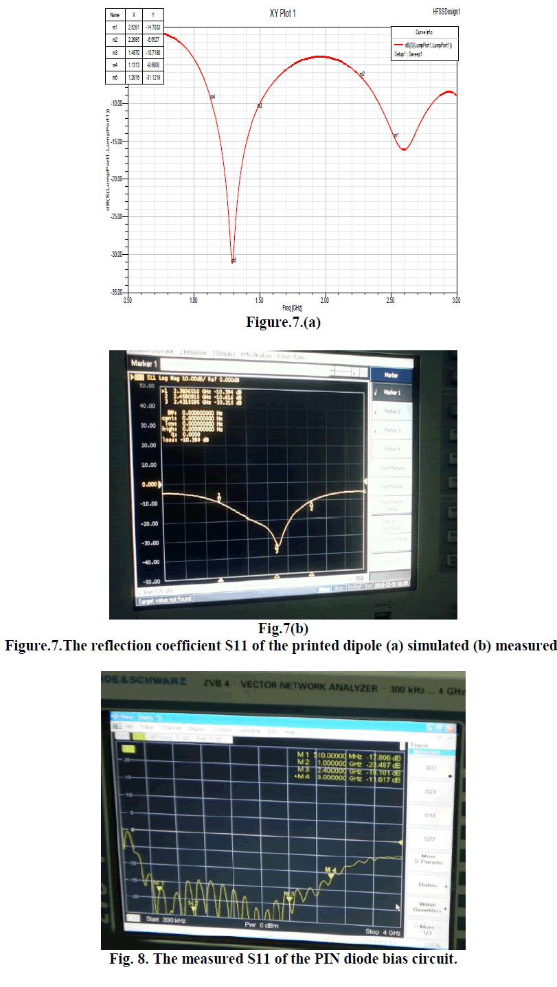
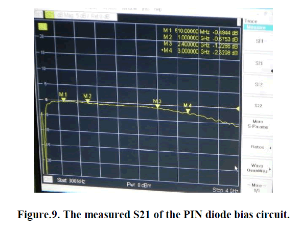
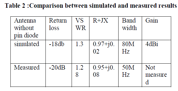
| The complete far-field radiation pattern as shown in figure (6) or response at a specific frequency can be determined by the near-to-far-field transformation method[4]. The VSWR of the printed dipole antenna with a via-hole balun is approximately lower than two from 2.2 to 2.9 GHz, with a bandwidth of approximately 80MHz. Figure (7) & (8) below shows the computed and measured return loss with good agreement. Figure(9) shows insertion loss of pin diode circuit as -1.2dB. |
 |
 |
 |
| The table (2) below shows the comparison between the simulated and measured results obtained for the printed dipole at 2.4GHz. |
 |
VI. CONCLUSION
|
| The proposed implementation represents a printed dipole antenna configuration for wireless applications at the frequency range of 2.4GHz. 60MHz impedance bandwidth is achieved practically with -25db return loss @ center frequency. Variations on the radiation pattern are observed due to presence pin diode active circuit. PIN diode are biased using 3 V & 10 mA. The proposed antenna can produce linear polarization and switch According to bias condition. The insertion loss is -2.8dB the conversion efficiency get compromised. The insertion loss of pin diode circuit is -0.9db. The total size of antenna is compatible for portable wireless application with the diversity features. |
References
|
- B. Edward and D. Rees, (1987) “A broadband printed dipole with integrated balun,” Microwave Journal, vol. 30, no. 5, pp. 339–344, 1987.
- B. G. Duffley, G. A. Morin, M. Mikavica, and Y. M. M. Antar,(2004) “A wide-band printed double-sided dipole array,” IEEE Transactions onAntennas and Propagation, vol. 52, no. 2, pp. 628–631
- C. Votis, V. Christofilakis, and P. Kostarakis, (2010) “Geometry aspects and experimental results of a printed dipole antenna,” InternationalJournal of Communications, Network and System Sciences, vol. 3, pp. 97–100
- G. S. Hilton, C. J. Railton, G. J. Ball, A. L. Hume, and M. Dean, (1995) “Finite-difference time domain analysis of a printed dipole antenna,”in Proceedings of the 9th International Conference on Antennas and Propagation, pp. 72–75, Eindhoven, The Netherlands.
- Huey-Ru Chuang, Member, IEEE, and Liang-Chen Kuo, Student Member, IEEE(2002) „âÃâ¬ÃŸ3-D FDTD Design Analysis of a 2.4-GHzPolarization-Diversity Printed Dipole Antenna With Integrated Balun and Polarization-Switching Circuit for WLAN and WirelessCommunication ApplicationsâÃâ¬ÃŸÃ¢Ãâ¬ÃŸ.
- M. C. Bailey,(1984) “Broad-band half-wave dipole,” IEEE Transactions on Antennas and Propagation, vol. 32, no. 4, pp. 410–412, 1984.
- Oliver Schmitz, Sven Karsten Hampel, Ilona Rolfes, Hermann Eul (2007) Impact of Sievenpiper High Impedance Surfaces on the Performanceof Planar Cross-Dipole Polarization Diversity Antennas.
- Won-Sang Yoon, Jung-Woo Baik, Member, IEEE, Hun-Sung Lee, SeongminPyo, Student Member, IEEE, Sang-Min Han, Senior Member,IEEE,and Young-Sik Kim, Member, IEEE(2010)A Reconfigurable Circularly Polarized Microstrip Antenna With a Slotted Ground Plane.
- Z. Fan, L. Ran, and K. Chen,(2005) “Printed dipole antenna designed with microstripbalun on v-shaped ground plane,” in Progress InElectromagnetic Research Symposium, pp. 23–26, Hangzhou, China, 2005.
- “Wireless communication principles and practices” by T.S. Rappaport.
- HSMP-389x Series, HSMP-489x Series Data sheet by Avago Technologies.
|