Keywords
|
| charge pump, loop filter, process , voltage and temperature (PVT), ring oscillator, voltage controlled oscillator. |
I. INTRODUCTION
|
| Phase locked loops (PLLs) are essential building blocks for almost all integrated Circuits. A Phase-locked loop (PLL) is the most widely used mixed-signal circuit block in a system-on-chip. Advancements in CMOS process technology have enabled circuits to be realized at low power and high performance. But, along with these advantages there exist a number of undesirable traits, such as a high degree of process and temperature variability, high leakage, and low dynamic range due to low supply voltage. This paper discusses the impact of these effects in designing Phase-Locked Loops in Nanometer CMOS. |
| Continuous scaling poses several design challenges for future high performance architectures. Systematic and random variations in process, supply voltage and temperature (PVT) have become a major challenge to future high performance architecture designs. Two main contributors to on chip variability arise from changes in process parameters and changes in operating temperatures. |
| VCO is the most important block of the PLL. Since area is dominated by the size of the inductor, LC oscillator does not scale well with technology. Therefore, we propose ring oscillator in our PLL design. Section (2) discusses the issues that are related to process and temperature compensated VCO. The free-running frequency of a ring oscillator is very sensitive to process, voltage and temperature (PVT). Process and Temperature compensation techniques for minimizing the variation of the free-running frequency of an oscillator are considered. |
| Charge pump and loop filter design is discussed in Section (3). The poor output conductance of short channel devices cause mismatch in the up and down currents. The effects of this on the PLL performance are discussed. Section (4) discusses the phase frequency detector cCircuit which offers zero dead zone with more number of transistors . Section (5) gives the simulation results of the PLL. |
II . VOLTAGE CONTROLLED OSCILLATOR
|
| In order to generate a precise frequency, this design is based on the voltage controlled ring oscillator and uses a process and temperature compensation bias technique to improve the oscillator’s immunity to environmental variations[4]. |
| A. Constant gm bias Circuit |
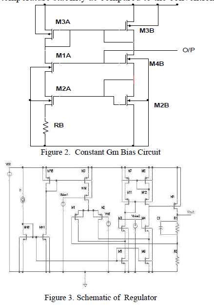
| Constant Transconductance (gm) bias circuits are widely used in many analog integrated circuit applications, such as low-noise amplifiers (LNA) and Gm−C filters. If the trans conductance and the reference voltage are process, voltage and temperature (PVT) independent then, naturally the current generated using these parameters is also PVT independent and hence can be used as a master bias current on a large analog chip. |
| Resistor-referred constant-gm bias circuit shown in Fig. 2 consists of differential pair with active current mirror[7] consisting of transistors M3A and M3B. While the transistors M1A, M2A , M2B and M4B constitute a cascade current mirror circuit which gives high impedance. The output from this circuit is taken from the drain of the transistor M 4B. |
| Assuming square-law devices and neglecting channel length modulation and body effect, this bias circuit provides a gm that is inversely proportional to resistor R. |
| B . Replica Circuit |
| The series-connected MOSFETS Mn and Mp |
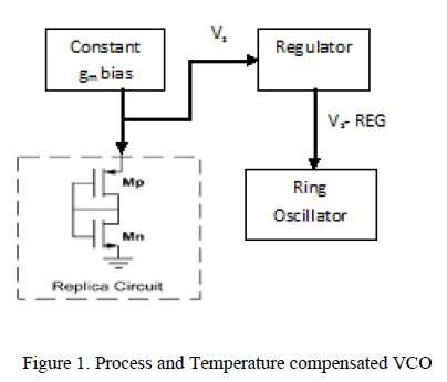
| generate the reference voltage for a regulator that powers the oscillator as shown in fig 1. |
| C. Voltage Regulator |
| The regulator should suppress external power supply noise to large frequencies and also filter out noise from the reference voltage such as that generated from the constant gm bias circuit. |
| These conflicting requirements in the Regulator Bandwidth can be met with two stage low-dropout (LDO) voltage regulator[5] for low-power applications is designed without an external capacitor for compensation. With the first stage being a wide band filter that offers good power supply rejection at high frequencies. And the second stage is a very narrow band stage that limits even flicker noise from reference that propagates to the oscillator. |
| The block diagram of process and temperature compensated VCO is shown in fig 1. |
 |
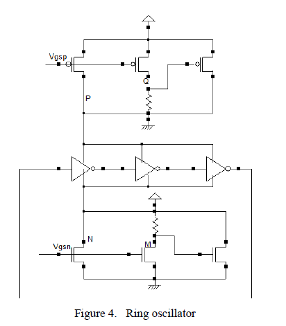
| The regulator has two stages as shown in fig 3, the first a folded cascode amplifier which allows a lot of gain to be obtained in a single stage consisting of PMOS transistors M1 and M2 which act as inputs, with transistors M9 and M10 forming the cascoded tail current source, and NMOS transistors M3 and M4 are the “folded back” common gate Transistors of the cascode. M5 and M6 provide the bias currents for M3 and M4 respectively. The folded cascode is Loaded by an improved Wilson current mirror, formed by M7, M8, M11, and M12 to improve output resistance of the stage and thus further increases the gain. |
| The second stage is a large pass transistor acting as a common-source amplifier. This device must be very wide so that it can source large load currents with a reasonable gate-source voltage. The output voltage of the LDO is at the drain of MP, and resistors R1 and R2 form a voltage divider to feed a fraction of the output voltage back to the input. Since the first stage is differential, it is less sensitive to power supply disturbances than the second stage, which is single-ended. |
| The PSRR of the LDO is 20 * log A2 /(1+A1 A2 Z) ] |
| Where A1 is gain of the first stage, A2 is the gain of the second stage and Z is feedback factor = R2/ (R1+ R2). |
| D. Ring Oscillator |
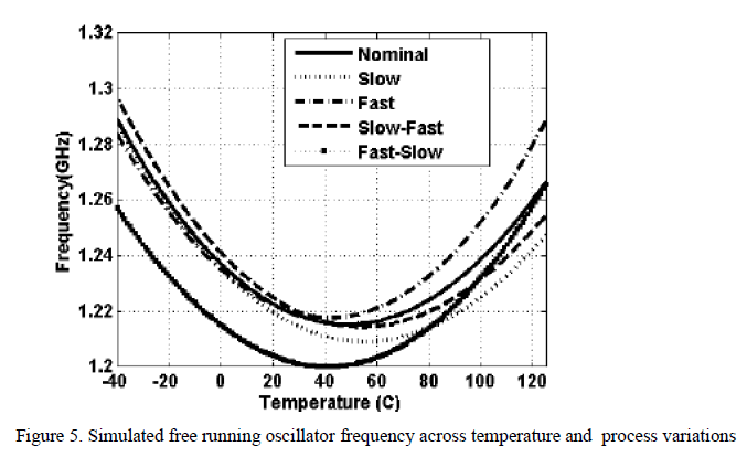
| An addition based current source ring oscillator presented in [9] shown in Fig 4. It is used to achieve 3x improvement in its frequency process variation and temperature stability as compared to the conventional current starved ring osillator. |
 |
| The nominal current provided by the top PFET current source is designed to match that of the bottom NFET currest source. M and N are two NFETs with the same width and length designed via a common centroid layout to obtain good local matching, so that the drain currents in both transistors will change in the same way when process conditions change. |
| Scalability is a desirable attribute for the current source when used as the bias current reference in ring oscillators, for it allows full integration with the digital processing circuits, which results in improved performance, reduced power and area, and higher oscillation frequency in newer processes. |
| There is only minimal additional phase noise contribution from the addition-based current source. At 10-MHz offset frequency, the spot phase noise is -103.87 dBc/Hz for the addition base ring oscillator. |
| The dominant parameters that are affected by process variations in a MOS transistor are channel mobility and threshold voltage. As the temperature increases, the mobility decreases, and the current from the constant-gm bias circuit increases. The threshold voltage has a negative temperature coefficient. The locally generated supply voltage for the oscillator will ensure that the Trans conductance of the n-channel devices at the quiescent point in the latch is held constant over process and temperature. |
 |
| Simulation results using a 0.18-μm technology are shown in Fig.5 for a nominal frequency of 1.25 GHz over a temperature range of −40âÃâæC to 125 âÃâæC for five process corners. The maximum frequency spread over process and temperature is about 100 MHz or within 55% of the nominal value. Fig 5 shows the measured free-running frequency from −40 âÃâæC to 125 âÃâæC, confirming the validity of the theory and simulations. The error bars show the spread over 15 devices. The addition-based ring oscillator dissipates 87μ W power on average and occupies 0.0128 mm2. |
III. CHARGE PUMP AND LOOP FILTER
|
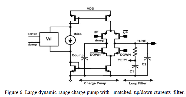
| The charge pump is another block that suffers from the low supply-voltage environment. In conventional charge pumps, the poor output conductance of short-channel devices causes mismatch in the up and down currents, as the output voltage deviates from the nominal value of half the supply voltage. In practice, the output voltage range is limited to a few hundred milli volts from either supply rail. Any attempt to drive the output past these limits causes significant mismatch in the up and down currents. This leads to increased reference spurs in the synthesized clock. The circuit shown in Fig.6 delivers very well matched up and down currents, even when the output is within a few tens of milli volts of the supply rails. |
| In figure 6, the charge pump circuit consists of two current mirrors with a differential amplifier placed between them. The upper current mirror produces the UP current which flows through the upper differential pair transistors and produces UP and UP1 signals. Similarly the lower current mirror produces the DOWN signal which flows through lower differential pair transistors and produces DOWN and DOWN1 signals. The output of the differential pair is given to TUNE in the circuit. While the other end of the output is given to the capacitor Cdump which is charged to Vdump. Voltage across the C2 capacitor is Vsense. |
 |
| When the PLL is close to lock, the up and down currents flow into dump capacitor Cdump for most of the reference period. Mismatch between these currents results in an effective nonzero average current, which charges or discharges Cdump The rail-to-rail V/I converter compares the voltages across Cdump and the loop filter sense node, and adjusts the currents Ibias until both voltages are equal and stable. This implies that the average currents into both the loop filter and Cdump must reach zero; this is a condition that is met only if the up and down currents are indeed corrected and made equal[1]. Op amp as comparator is used to compare Vsense and Vdump and give a single voltage to V to I Converter. |
| A two stage op amp is designed with a single ended output the first stage being a differential amplifier which provides high gain and the second stage provides large swings. The second stage is a simple common source stage so as to allow maximum output swings. |
| The capacitor C connected between Gate and Drain of the transistor M9 is in the feedback path, provides a feed forward path that conducts the input signal to the output at very high frequencies resulting in a slope in the frequency response. The main purpose of the capacitor is to improve the bandwidth. |
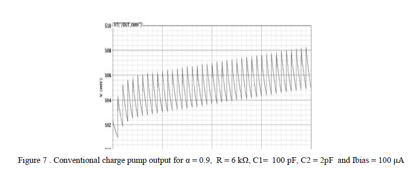
| A simple passive loop filter consists of a resistor R that is connected in series with a capacitor C1. The resistor influences the bandwidth of the loop, whereas the capacitor controls the damping. To save area, the capacitor may be realized by a MOS device, although it may have large voltage dependence. The capacitor C2 in fig.6 smoothes large IR ripple on Vcntrl. Fig 7 is output of charge pump. |
 |
 |
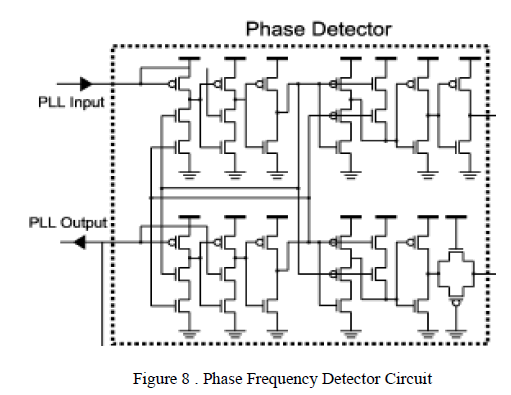
IV. PHASE FREQUENCY DETECTOR
|
| The conventional PFD consists of an AND gate and two DFFs. The DFF implementation, being an extensively studied topic, leads to many PFD design alternatives employing modified DFFs or latches for faster operation. |
| One of the disadvantages that PFD suffers is dead-zone. Dead-zone is a small difference in the phase of the inputs that a PFD will not be able to detect. Dead zone is due to the delay time of the logic components and rest of the feedback path of the flip flops. PFD with large dead zone would cause PLL output jittered and the locking time consumed. To minimize the effect of the finite dead zone, gain of PFD must be reduced when PLL is locked and hence a short charging or discharging time of the charge pump can be resulted. TSPC DFF is more used in designing DFF of PFD for supporting high speed operation. Double edge triggered DFFs deliver high performance and do not suffer from the problems of charge sharing, charge coupling, reduced voltage swing, poor supply voltage properties and excessive power dissipation plaguing existing DETFFs [8]. |
| Inverters are placed in the PFD to increase the output swing because as Vt is scaled down any circuit driven by a signal which does not achieve a rail to rail swing may experience static power dissipation. Circuits that do not show full swing will fail earlier because the supply voltage needs to be scaled down with the advancement of technology [2]. |
| The transistor sizes in DFF and AND gates were so small in micrometer and because the transistors are used in digital circuitry, the transistors could not switch enough at frequency of 100 MHz. Thus two inverters were placed at the outputs of the UP and DOWN signals in fig. 8 in order to make the signals go to discrete low and high levels ( or to improve the output swing). |
 |
V. SIMULATION RESULTS
|
| For all the blocks and sub blocks of the PLL, schematics are drawn with the help of cadence tools using TSMC library 90nm CMOS technology. An on-chip clock generation can be made by using a voltage controlled oscillator with a specific control voltage. Some bias techniques have been proposed to compensate for variations in either temperature or process. Hence we use a process and temperature compensation bias technique to improve the oscillators immunity to environmental variations. |
 |
VI. CONCLUSION
|
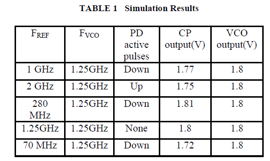
| In this paper temperature process compensated VCO with low power additional based ring oscillator and zero dead zone PFD for high performance PLL has been presented. The design is implemented in 90nm CMOS technology. The circuits are simulated on Virtuso Cadence tool with GPDK 90nm CMOS technology. The simulation results show that it operates well at high frequency of 1.25GHz with power supply voltage of 1.8V. The PFD designed has nearly zero dead zone. |
References
|
- Kadaba R. Lakshmikumar, “Analog PLL Design With Ring Oscillators at Low –Gigahertz Frequencies in Nanometer CMOS: Challenges andSolutions” IEEE Circuits and Systems-II, vol 56,no 5,pp 389-393, May 2009.
- Chu-Lung Hsu,Yiting Lai, Shu-Wei Wang ,“Built –in-Self –Test for Phase Locked Loops,” IEEE Instumentation& Measurement, vol 54,no 3, pp996-1002, June 2005.
- Won Hyo LEE, Sung Dae LEE, Jun-Dung CHO,”A High Speed , Low Power Phase Frequency Detector and Charge Pump circuits for HighFrequency Phase Locked Loops” IEICE Trans Fundamentals , vol E82-A, no 11, pp 2514-2519, November 1999.
- A. Hajimiri, S. Limotyrakis, and T. Lee, “Jitter and phase noise in ring oscillators,” IEEE J. Solid-State Circuits, vol. 34, no. 6, pp. 790–804,Jun.1999.
- Miranda J. Ha, “A Low-Power, High-Bandwidth LDO Voltage Regulator with No External Capacitor”, S.B. EE, M.I.T., 2007.
- K. Lakshmikumar, V. Mukundagiri, and S. Gierkink, “A process and temperature Compensated two-stage ring oscillator,” in IEEE CustomIntegr.Circuits Conf., Sep. 2007, pp. 691–694.
- B. Razavi, Design of Analog CMOS Integrated Circuits McGraw-Hill, 2001.
- Kiat-Seng Yeo, Samir S .Rofail, Wang –Ling Goh , CMOS/ BiCMOS ULSI Low Voltage, Low Power Pearson Education, 2002.
- Xuan Zhang, Student Member, IEEE, and Alyssa B. Apsel, Member, IEEE. A Low-Power, Process-and-Temperature-Compensated Ring OscillatorWith Addition-Based Current Source.
|