Keywords
|
| Photovoltaic controller(PV), Cascaded Cockcroft Walton (CCW), Voltage multiplier. |
INTRODUCTION
|
| The paper is about stand-alone photovoltaic generation system. The word stand-alone refers to the fact that the system works without any connection to an established power grid. Stand-alone PV systems are autonomous power grids being supplied with energy from a photovoltaic generator. Examples of such systems include electricity supply systems on islands, for isolated settlements or entire villages. The PV generator as the source of renewable energy is the crucial component of the stand-alone power system. Stand-alone power systems are generally differentiated according to their type of voltage (DC or AC). In DC coupled systems, the PV generator is connected via a special DC/DC converter. As in [2] dc-dc converter employs a transformer for voltage boost up using an asymmetrical pulse width modulation technique. So suitable isolation circuitry is sufficient for effective operation of the circuit. In order to overcome this complexity of the circuit a converter using multiplier units are employed for voltage boost up. The battery or standalone power inverter is the heart of the AC coupled system. It ensures that generated and load power are balanced at all times. If too much energy is generated, the inverter stores this surplus energy in the batteries. If energy demand exceeds supply, the inverter discharges energy from the batteries. If the load is to be supplied independently of solar insolation, the generated power is stored and buffered with a battery. In non-portable applications where weight is not an issue, such as in buildings, lead acid batteries are most commonly used for their low cost and tolerance for abuse. A photovoltaic (PV) system may be a combination of several components such as a battery system, DC/AC conversion circuits, and other power conditioning devices in addition to the solar panels themselves. A photovoltaic generator is the whole assembly of solar cells, connections, protective parts, supports etc. A photovoltaic system uses one or more solar modules or panels to convert solar energy to electrical energy. |
DC-DC CONVERTER
|
| A renewable power generation system using a photovoltaic controller circuit with a high step-up dc-dc booster converter based on the Cockcroft-Walton (CW) voltage multiplier without a step-up transformer is being discussed here. Providing continuous input current with low ripple, high voltage ratio, and low voltage stress on the switches, diodes, and capacitors, by cascading suitable multiplier cells. The proposed converter is quite suitable for applying to low-input-level dc generation systems. Moreover, based on the n-stage CW voltage multiplier, the proposed converter can provide a suitable output with a voltage boost up required for high power applications. The control strategy employs two independent frequencies, one of which operates at high frequency of 60KHz to minimize the size of the inductor while the other one operates at relatively low frequency of 1 KHz according to the desired output voltage ripple. |
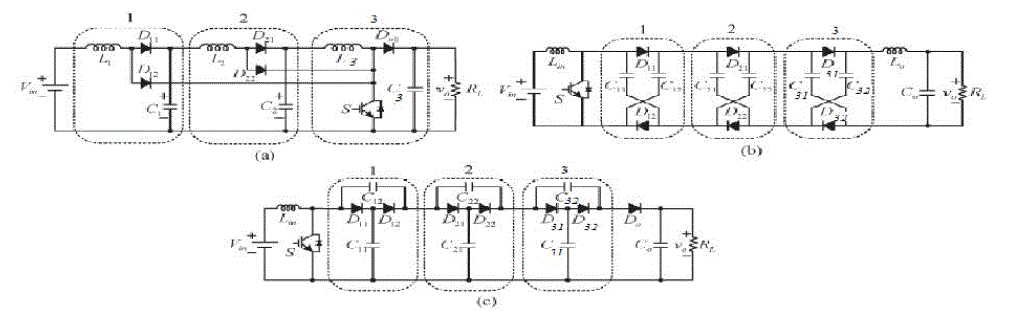 Fig.1. Different Cascaded Converter Fig.1. Different Cascaded Converter |
| Figure given above shows a three stage cascade boost converter with different topologies proposed for obtaining a high voltage gain. Figure 1(a) shows a 3-stage cascade boost converter proposed in [3] for obtaining a high voltage gain. However, the passive elements and switch sustained high voltage stress in this cascaded converter. Some other structures with switched-capacitor or switched-inductor circuits combined with basic transformerless topologies were also discussed. Figure 1(b) shows another topology as in [4], which consists of a conventional boost converter and a diode capacitor multiplier. The main advantage of this topology is that higher voltage gain can easily be obtained by adding the stages of the diode-capacitor multipliers without modifying the main switch circuit. Nevertheless, the voltage across each capacitor in each switched capacitor stage goes higher when a higher stage converter is used. Figure 1(c) shows another similar topology [5] which has advantages similar to that of the topology in [6]. However, the voltage stress on the capacitors of higher stage is still rather high. Moreover, a modified topology, with integrated interleaved multiphase boost converter and voltage multiplier, was proposed here for high-power applications as well. In this topology, all capacitors in the voltage multiplier have identical voltage which is equal to VO / (n + 1). In order to simplify the analysis of circuit operation, the proposed converter with a three stage CW voltage multiplier is used. Before analyzing, all of the circuit elements are ideal, and there is no power loss in the system. Figure 2 is the proposed converter with three- stage CW voltage multiplier. When a high-frequency periodic alternating current is fed into the circuit and all of the capacitors in the CW voltage multiplier are sufficiently large, the voltage drop and ripple of each capacitor voltage can be ignored under a reasonable load condition[7]. Thus, the voltages across all capacitors are equal, except the first capacitor whose voltage is one half of the others. The proposed converter is operating in CCM and in the steady-state condition. When the inductor transfers the storage energy to the CW circuit, only one of the diodes in the CW circuit will be conducted. |
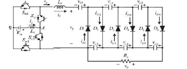 Fig.2. Proposed three stage CW converter Fig.2. Proposed three stage CW converter |
| A high step-up converter based on the CW voltage multiplier is proposed by replacing the step-up transformer with the boost-type structure, and thereby provides higher voltage ratio than that of the conventional CW voltage multiplier. Thus, it is suitable for power conversion applications where high voltage gains are desired. Moreover, the converter operates in continuous conduction mode (CCM), so the switch stresses, the switching losses, and EMI noise can be reduced as well. The proposed converter deploys four switches, in which Sc1 and Sc2 are used to generate an alternating source to feed into the CW voltage multiplier and Sm1 and Sm2 are used to control the inductor energy to obtain a boost performance. This will increase the complexity and cost of the proposed converter because an isolated circuit is necessary to drive the power semiconductor switches. |
SIMULATION STUDY
|
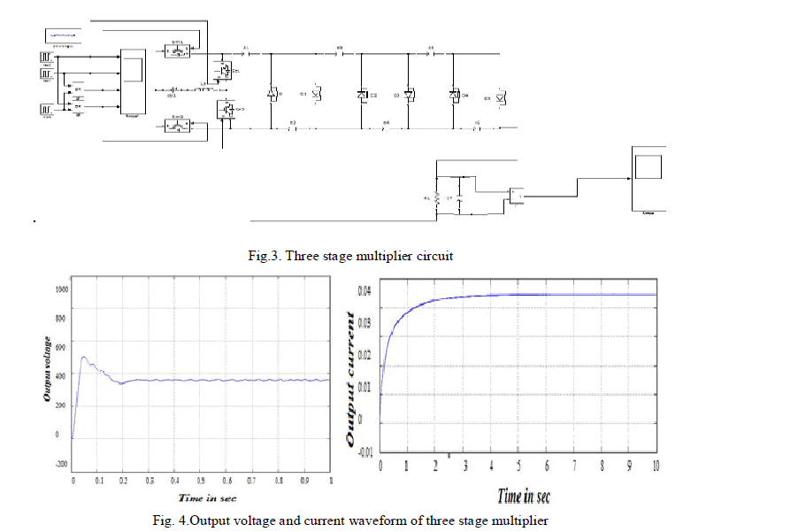
| A. 3-Stage multiplier circuit |
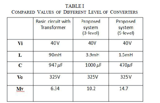
| The MATLAB 2009b simulation model of a three stage voltage multiplier is shown in figure 3. Here multiplier circuit using three set of diode capacitor combination is shown for voltage boost up instead of a transformer. The capacitor used is of 1000μF and the inductor is of 3.9mH. As for the given input voltage of 40 voltage, an output voltage boost up upto 325 volt and current of .03A is obtained and is shown in figure 4. For the given value of capacitance and inductance , a gain of 10.2 is obtained. |
 |
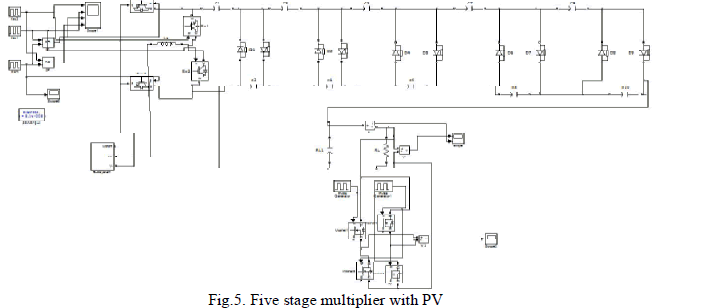
| B. 5-Stage Multiplier with PV |
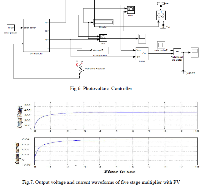
| The simulation circuit of a five stage voltage multiplier using photovoltaic controller is shown in figure 5. Here a multiplier circuit uses five capacitors and five diodes for voltage boost up instead of a transformer. Here the input voltage applied is generated by means of a Photovoltaic module as shown in figure 6, instead of giving a direct DC input voltage. Since the voltage generated by the PV is not much suitable for high power applications it should have to be converted to high power by means of multiplier circuit. |
| Here also for a given input voltage of 40 voltage, generated by photovoltaic module is given, and thereby a boost up upto 325 volts is obtained with a capacitor rating of 470μF and inductance of 1.5 mH. The obtained DC output voltage is further converted to AC to complete the controller circuit. As for the given input voltage of 40 voltage, an output voltage boost up upto 325 volt and current of 0.065 A is obtained and is shown in figure 7. |
 |
 |
| E. Comparative Study |
| Cascaded voltage multiplier cell with three stage and five stage voltage multiplier is discussed above. As for both three stage and five stage same voltage boost up upto 325V can be obtained by using different values of capacitance and inductance. By reducing the value of inductance from 3.9mH to 1.5mH and capacitance from 1000μF to 470μF the voltage boost up is same for five stage as in case of three stage. Also by using the five stage multiplier the voltage can be boost up from that obtained from three stage, since five multiplier unit is present instead of three. There by the gain can be improved by 2% . |
 |
HARDWARE DETAILS
|
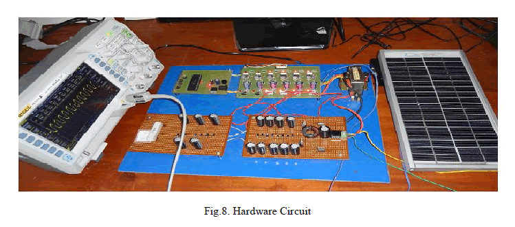 |
| An experimental prototype has been built to verify the performance of the proposed converter as shown in the figure 8. An MPPT controller implemented in a microcontroller will provide a reference voltage Vpv ref that will be used by the dc/dc controller to determine the converters operation mode. The dc/dc controller will check Vpv and Ppv every few minutes. The controller circuit used here includes a PIC microcontroller. A center tapped transformer is used in the rectifier stage and the input voltage is assumed to be supplied from a preregulator. |
| A DC-DC converter with a 200W output has been selected for design. According to the design guidelines, the prototype was implemented. Compared with a discrete MOSFET and PWM controller solution, the Fairchild -series can reduce total cost[12], component count, size, and weight, while simultaneously increasing efficiency, productivity, and system reliability. The circuit for the experimental testing shows the references of the MOSFET, diodes and driver that were used in to construct the circuit, and also shows the values of the elements and voltage sources. The figure given above shows full bridge converter driven by the PWM controlled driver circuit. The values of the inductors were changed, because the first inductors were very large, although when this change it was taken into account that the ripples of the input current continued to be low. The inductors were designed using the Magnetics Inductor Design using Powder Cores Software. This software uses a design algorithm intended to specify the smallest design package size for the given input parameters (currents, inductance values, frequency, etc.). It also provides the values for the parasitics that will be used in the simulations of the circuit prototype. MMK technology capacitors were used because of their good characteristics. |
| A. Experimental Results |
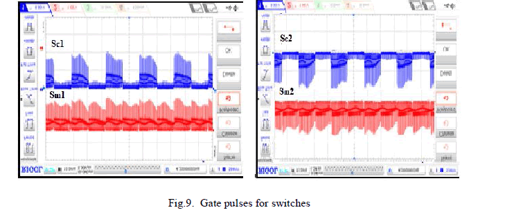
| A prototype with 200 W rating was built to verify the validity of the proposed converter. Some waveforms of the proposed converter at Po = 200 W, Vin = 40 V, and Vo = 325 V for experiment is shown here. Figure 9 shows the switching signals for the four switches, in which Sc1 and Sc2 are operated at fsc at lower frequency of 1KHz and Sm1 and Sm2 are operated at a higher frequency fsm of 60KHz. |
 |
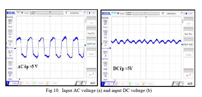
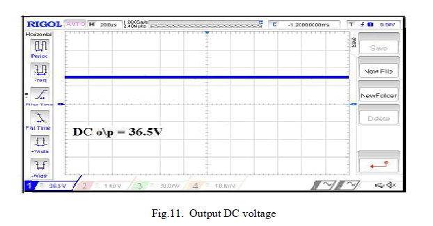
| Moreover, the results of the input voltage , and the output voltage Vo of the CW voltage multiplier are shown in the figure 10 and figure 11 respectively. Obviously, the simulation results will agree with the experimental results. In theoretical analysis, the input current ripple frequency (fsc) is ignored due to the fact that the capacitors are assumed large enough to obtain stable capacitor voltages with no voltage ripple in the CW voltage multiplier. However, the voltage ripple exists practically in all capacitors. In other words, the input current and the output voltage have the same ripple frequency (fsc). |
 |
| For an input dc voltage of 5V, the voltage boost up upto 36V is obtained. Here a booster circuit with seven stages of cascaded converter with capacitor diode combination is employed in the hardware section. With this the voltage multiplication is possible, for each diode capacitor combinations twice the voltage boost up may occur. The output of the proposed converter is regulated at 325 V, thus the voltage gains corresponding to these input voltages for five and seven stages can be obtained. The results represent that the proposed converter has lower efficiency at lower input because of higher conducting loss accompanied by higher input current. On the other hand, for higher load condition, the efficiency decreases due to the conducting loss of the diodes and the resistance loss of the capacitors. |
 |
CONCLUSION
|
| A typical solar panel converts only 30 to 40 percent of the incident solar irradiation into electrical energy. Maximum power point tracking technique is used to improve the efficiency of the solar panel. At a given temperature and illumination level, solar cells supply maximum power at one particular voltage and current output called the maximum power point. The generated power is not much applicable to high power applications, so that it should be boost up to required level by means of suitable converter. |
| A high step- up dc-dc converter based on the cascaded voltage multiplier without a line- or high-frequency step up transformer has been presented to obtain a high voltage gain. Since the voltage stress on the active switches, diodes, and capacitors is not affected by the number of cascaded stages, power components with the reduced voltage ratings can be selected. The circuit operation, design considerations, and control strategy were discussed. The proposed control strategy employs two independent frequencies, one of which operates at high frequency of 60KHz to minimize the size of the inductor while the other one operates at relatively low frequency of 1KHz according to the desired output voltage ripple. Finally, the simulation and experimental results proved the validity of theoretical analysis and the feasibility of the proposed converter. In future work, the influence of loading on the output voltage of the proposed converter will be derived for completing the steady-state analysis. |
References
|
- M. Prudente, L. L. Pfitscher, G. Emmendoerfer, E. F. Romaneli, and R. Fules, “Voltage multiplier cells applied to non-isolated DC-DC con-verters,” IEEE Trans.Power Electron., vol. 23, no. 2, pp. 871–887, Mar. 2008.
- R.J.Wai,C.Y.Lin,R.Y. Duan, and Y. R. Chang, “High-efficiency DC–DC converter with high voltage gain and reduced switch stress,” IEEE Trans. Ind. Electron.,vol. 54, no. 1, pp. 354–364, Feb. 2007.
- Hyun-Lark Do Zhang , “Asymmetrical full bridge converter with high- voltage gain”, in Proc. IEEE Transactions on Power Electronics, vol.27, no 2 ., Feb. 2012.
- Chung-Ming Young, Member, IEEE, Ming-Hui Chen, Student Member, IEEE, Tsun-An Chang, Chun-Cho Ko, and Kuo-Kuang Jen “Cascade Cockcroft–WaltonVoltage Multiplier Applied to Transformerless High Step-Up DC–DC Converter,” IEEE Trans. Ind. Electron., vol. 60, no. 2, February 2013.
- T. F. Wu, Y. S. Lai, J. C. Hung, and Y. M. Chen, “Boost converter with coupled inductors and buck-boost type of active clamp,” IEEE Trans. Ind. Electron., vol.55, no. 1, pp. 154–162, Jan. 2008.
- S. S. Lee, S. W. Rhee, and G. W. Moon, “Coupled inductor incorporated boost half-bridge converter with wide ZVS operation range,” IEEE Trans. Ind. Electron.,vol. 56, no. 7, pp. 2505–2512, Jul. 2009.
- C. S. Leu, P. Y. Huang, and M. H. Li, “A novel dual-inductor boost converter with ripple cancellation for high-voltage-gain applications,” IEEE Trans. Ind.Electron., vol. 58, no. 4, pp. 1268–1273, Apr. 2011.
- L.-S. Yang, T.-J. Liang, and J.-F. Chen, “Transformerless DC-DC converters with high step-up voltage gain,” IEEE Trans. Ind. Electron., vol. 56, no. 8, pp. 3144–3152, Aug. 2009
- Q. Zhao, F. Tao, Y. Hu, and F. C. Lee, “Active-clamp DC/DC converter using magnetic switches,” in Proc. IEEE Appl. Power Electron. Conf. Expo., 2001, pp.946–952.
- E. Adib and H. Farzanehfard, “Zero-voltage transition current-fed fullbridge PWM converter,” IEEE Trans. Power Electron., vol. 24, no. 4, pp. 1041–1047, Apr.2009.
- M. M.Weiner, “Analysis of Cockcroft–Walton voltage multipliers with an arbitrary number of stages,” Rev. Sci. Instrum., vol. 40, no. 2, pp. 300–333,Feb. 1969.
- E. AdibH. van der Broeck, “Analysis of a current fed voltage multiplier bridge for high voltage applications,” in Proc. IEEE PESC, 2002, pp. 1919- 1924
|