International Journal of Advanced Research in Electrical, Electronics and Instrumentation Engineering
ISSN ONLINE(2278-8875) PRINT (2320-3765)
ISSN ONLINE(2278-8875) PRINT (2320-3765)
Saradindu Panda1, A.Banerjee2 B.Maji3, Dr.A.K.Mukhopadhyay4
|
| Related article at Pubmed, Scholar Google |
Visit for more related articles at International Journal of Advanced Research in Electrical, Electronics and Instrumentation Engineering
This paper describes the speed of the design is limited by size of the transistors, parasitic capacitance and delay in the critical path. Power consumption and speed are two important but conflicting design aspects; hence a better metric to evaluate circuit performance is power delay product (PDP).The driving capability of a full adder is very important, because, full adders are mostly used in cascade configuration, where the output of one provides the input for other. If the full adders lack driving capability then it requires additional buffer, which consequently increases the power dissipation. Here, we have given a brief description of the evolution of full adder circuits in terms of lesser power consumption, higher speed and lesser chip size. We have started with the most conventional 28 transistor full adder and then gradually studied full adders consisting of as less as 8 transistors. We have also included some of the most popular full adder cells like Static Energy Recovery Full Adder (SERF) [7] [8], Adder9A, Adder9B, GDI based full adder.
Keywords |
| CMOS Transmission Gate (TG), Pass-Transistor Logic (PTL), Complementary Pass-transistor Logic (CPL), Gate Diffusion Input (GDI), Static Energy Recovery Full Adder (SERF), Adder9A, Adder9B, GDI based full adder Power, Delay, Channel Length. |
I. INTRODUCTION |
| The extensive development in the field of portable systems and cellular networks has intensified the research efforts in low power microelectronics. The low-power design has become a major design consideration. The design criterion of a full adder cell is usually multi-fold. Transistor count is, of course, a primary concern which largely affects the design complexity of many function units such as multiplier and algorithmic logic unit (ALU). The limited power supply capability of present battery technology has made power consumption an important figure in portable devices. |
| The speed of the design is limited by size of the transistors, parasitic capacitance and delay in the critical path. The driving capability of a full adder is very important, because, full adders are mostly used in cascade configuration, where the output of one provides the input for other. If the full adders lack driving capability then it requires additional buffer, which consequently increases the power dissipation. In the last decade, the full adder has gone through substantial improvement in power consumption, speed and size, but at the cost of weak driving capability and reduced voltage swing. However, reduced voltage swing has the advantage of lower power consumption [3]. |
| There is no ideal full adder cell that can be used in all types of applications [4]. Hence novel architectures such as CMOS Transmission Gate (TG), Pass-Transistor Logic (PTL), Complementary Pass-transistor Logic (CPL) [5] and Gate Diffusion Input (GDI) [6] are proposed to meet the requirements. Each design style has its own share of advantages and disadvantages. Gate Diffusion Input is a low power design that reduces transistor count. But the major problem of GDI is that it requires twinwell CMOS or silicon on insulator (SOI) process for fabrication [11]. Thus GDI chips are more expensive. These logic styles and their combinations (Hybrid) are commonly used in designing full adder cells. |
| In this paper, we have given a brief description of the evolution of full adder circuits in terms of lesser power consumption, higher speed and lesser chip size. We have started with the most conventional 28 transistor full adder and then gradually studied full adders consisting of as less as 8 transistors. We have also included some of the most popular full adder cells like Static Energy Recovery Full Adder (SERF) [7] [8], Adder9A, Adder9B, GDI based full adder. |
II. TRUTH TABLE AND EQUATION |
| A full adder performs the addition of two bits A and B with the Carry (Cin) bit generated in the previous stage. The integer equivalent of this relation is shown by: |
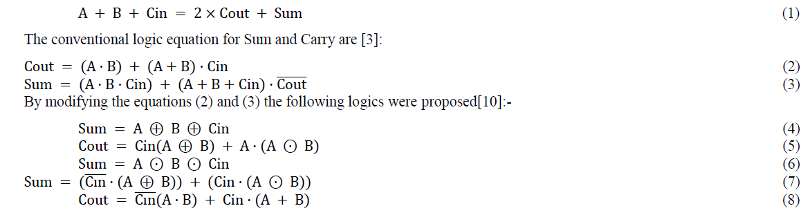 |
| Full Adder using CMOS Logic and will be called as “Conventional CMOS design”. The block diagram of conventional CMOS Full Adder is shown below (Fig 1): |
III. MEASUREMENT COMPARATIVE ANALYSIS OF DIFFERENT TYPES OF FULL ADDER CIRCUITS |
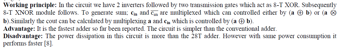
| A. CONVENTIONAL 28T CMOS FULL ADDER: |
| This adder was based on regular CMOS structure (pull-up and pull-down network) (Fig 2). |
| Working principle: Cout is generated first using equation 3. Then the sum is derived from the sum using equation 4. |
| Advantages: One of the most significant advantages of this full adder was its high noise margins and thus reliable operation at low voltages. The layout of CMOS gates was also simplified due to the complementary transistor pairs. |
| Disadvantages: But the use of substantial number of transistors results in high input loads, more power consumption and larger silicon area. |
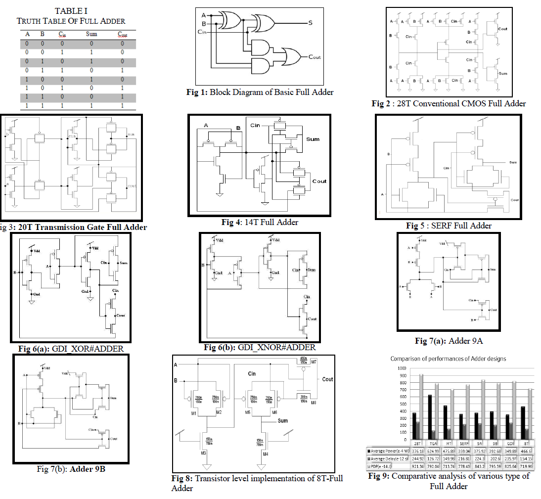
| B. 20 T TRANSMISSION GATE FULL ADDER: |
| It produces buffered outputs of proper polarity for both sum and carry with the disadvantage of high power consumption. (Fig.3). |
 |
| C. 14T FULL ADDER: |
| The 14T full adder contains a 4T PTL XOR gate, shown in Fig. 4, an inverter and two transmission gates based multiplexer designs for sum and Cout signals[11]. |
| Working principle: This circuit has 4 transistor XOR which in the next stage is inverted to produce XNOR. These XOR and XNOR are used simultaneously to generate sum and cout. The signals cin and ÃÅÃ⦠ÃÅÃ⦠ÃÅÃ⦠ÃÅÃ⦠are multiplexed which can controlled either by (a b) or (a b). Similarly the cout can be calculated by multiplexing a and cin controlled by (a b). |
| Advantage: It is the fastest adder so far been reported. The circuit is simpler than the conventional adder. |
| Disadvantage: The power dissipation in this circuit is more than the 28T adder. However with same power consumption it performs faster [4]. |
| D. 10T STATIC ENERGY RECOVERY FULL ADDER: |
| In this type of adder (Fig 5) the energy recovering logic reuses charge and therefore consumes less power than non-energy recovering logic. |
| Working principle: The circuit consists of two XNORs realized by 4 transistors. Sum is generated from the output of the second stage XNOR circuit. The cout can be calculated by multiplexing a and cin controlled by (a ⊗ b). Let us consider that there is a capacitor at the output node of the first XNOR module. To illustrate static energy recovery let us consider an example where initially a=b=0 and then a changes to 1. When a and b both equals to zero the capacitor is charged by VDD. In the next stage when b reaches a high voltage level keeping a fixed at a low voltage level, the capacitor discharges through a. Some charge is retained in a. Hence when a reaches a high voltage level we do not have to charge it fully. So the energy consumption is low here. |
| Advantage: It should be noted that the new SERF adder has no direct path to the ground. The elimination of a path to the ground reduces power consumption. The charge stored at the load capacitance is reapplied to the control gates. The combination of not having a direct path to ground and the re-application of the load charge to the control gate makes the energy-recovering full adder an energy efficient design[12]. |
| Disadvantage: The circuit produces full-swing at the output nodes. But it fails to provide so for the internal nodes. As the power consumption by the circuit reduces the circuit becomes slower. Also it cannot be cascaded at low power supply due to multiple threshold problems [12]. |
| E. 10T FULL ADDERS REALIZED BY GATE DIFFUSION INPUT (GDI) STRUCTURES: |
| Now using these GDI based XOR and XNOR gates two different GDI based full adder architecture were designed [Fig. 6]. |
| Circuit Operation: The circuit operation of GDI Based Full Adders is exactly the same as that of previous SERF module. Sum bit is obtained from the output of the second stage of XOR [Fig. 6(a)], XNOR [Fig. 6(b)] circuit while Carry bit (Cout) is calculated by multiplexing B and Cin controlled by (A XNOR B). |
| Advantage: These features give the GDI cell two extra input pins to use which makes it flexible than usual CMOS design. It is also a genius design which is very power efficient without huge amount of transistor count. |
| Disadvantage: The major problem of a GDI cell is that it requires twin-well CMOS or silicon on insulator (SOI) process to realize. Thus, it will be more expensive to realize a GDI chip. Moreover if only standard p-well CMOS process is used, the GDI scheme will face the problem of lacking driving capability which makes it more expensive and difficult to realize as a feasible chip. |
| F. ADDER 9A AND 9B: |
| Working Principle: From the above figures (Fig 7a and 7b), we can see that a Static Energy Recovery XNOR gate is cascaded with the new G-XNOR gate to generate the Sum while the Cout function is implemented by simply multiplexing B and Cin controlled by (A XNOR B) as done in the previous circuits. |
| Advantage: These two new adders consistently consume less power in high frequencies and have higher speed compared with the previous 10-transistor full adders and the conventional 28-transistor CMOS adder [13]. |
| G. DESIGN OF 8T FULL ADDER: |
| The basic of 8T full adder consists of 3 modules: 2 XOR elements and a Carry section as shown in figure below: |
| Working Principle:The Sum output is obtained by two XOR blocks in succession. For the carry section we use GDI based 2TMUX and (A XOR B)as the selection signal. The Sum and the Cout module need 6 and 2 transistors respectively. The transistor level implementation of the eight transistor full adder is shown in Fig. 8. It is obvious from the figure that both Sum and Cout has a maximum delay of 2T. |
| Advantage: It doesn’t suffer from threshold voltage loss problem. Also the noise margin has been substantially increased by proper sizing of transistors in 3T XOR. The power delay product (PDP), and the area of the proposed adder are also found better than that of the existing 10T and 14T adders. |
| Disadvantage: Higher power consumption due to short circuit current. |
 |
IV. RESULT ANALYSIS |
| Comparative analysis between various type of Full Adder is shown in Fig: 9. |
V. CONCLUSION |
| From the analysis of the above various type of Full Adder Circuits we can reach to a conclusion that the average power is low for GDI type Full adders and Average Delay is low for TG Based Full Adder. But the Power Delay Product is low for 14T Full Adder. But Power dissipation is higher than 8T Full Adder. For Optimization of Power (Average power) and Delay, we think that the best option is 8T Full Adder. |
| Full Adders is the heart of any digital processor. Here we have shown the implementation of various type of Full Adders using MOSFET. However recent researches have shown that Carbon-Nano-Tubes have a huge potential in logic circuits. Not only will it reduce power consumption, but also increase speed substantially. |
ACKNOWLEDGMENT |
| The authors would like to thank Prof. (Dr.) M.R.Kanjilal and Faculty Members, Department of Electronics and Communication Engineering, Narula Institute of Technology, WBUT, for many insightful discussions. |
References |
|