International Journal of Advanced Research in Electrical, Electronics and Instrumentation Engineering
ISSN ONLINE(2278-8875) PRINT (2320-3765)
ISSN ONLINE(2278-8875) PRINT (2320-3765)
B.BalaBhuvanapriya1, S.Janani1
|
| Related article at Pubmed, Scholar Google |
Visit for more related articles at International Journal of Advanced Research in Electrical, Electronics and Instrumentation Engineering
In this paper, the main aim of this project is design the low power VLSI technology. The reason for the power dissipation is switching activity in the circuit. In base paper they used Dual Mode One Latch Double Edge Triggered Scan flop for reducing the switching activity. If switching activity reduces means the power dissipation will also reduce. Scan flop is nothing but combination of D-Flip flop and Multiplexer. The scan flops are combining with shift register to form a scan chain. The scan chains are used to make the testing operation in easy manner. Dual mode one latch double edge triggered is used to reduce the multi cycle path constraints. Due to the reduction of switching activity the power dissipation and time delay will reduce. But this method is older. Nowadays lot of technologies is invented. From that two methods are used. One is Gated logic circuit and Precomputation method. In Gated logic method the AND gate will be use in scan flop for reducing the power effectively. And in precomputation method comparators are used with scan chain.
Keywords |
| Scan flop, Scan chain, DOL-DET |
I.INTRODUCTION |
| Power consumption in scan based testing is high due to the toggling of the combinational logic during the scan shift. Here a modified Scan Flip-flop architecture with a minimal area overhead which completely eliminates the switching power dissipation and also reduces the leakage power in the combination circuit during the shift phase of a scan based test. This also enables us to increase the shift frequency since power is no longer a limiting factor during scan shift and help in achieving test time reduction. |
| Testing of VLSI circuits can lead to generation of excessive heat which can damage the chips under test. In scan based testing methodology, high-performance CMOS circuits consume significant dynamic power during testing because of enhanced switching activity. The power and energy consumption of digital systems may increase significantly during testing. This extra power consumption during test application may reduce circuit reliability. The consumed energy directly corresponds to the switching activity generated in the circuit during test application. This has an impact on battery lifetime during remote self-testing. Test-per-scan techniques involve applying test patterns from a loaded scan chain to a circuit under test (CUT) every m+1 clock cycles, where m is the number of flip-flops in the scan chain. Most of the power-dissipation in the CUT will occur during the shifting of bits into the scan chain. The two types of power consumption that are of importance, during test mode of a circuit, are peak power and average power. |
| The main motivation for considering power consumption during test application is that power and energy of a digital system can be considerably higher in test mode than in system mode. The reason is that test patterns can cause many combinational nodes switch while a power saving system mode only activates a few modules at the same time. Another reason is that successive functional input vectors applied to a given circuit during system mode have a significant correlation. There is no specific correlation between the consecutive test patterns generated by an ATPG tool (for external testing) or that created by an LFSR (for BIST) for testing such circuits. This can cause considerably larger switching activity in the circuit during test than during its normal operation. Since power dissipation in CMOS circuits is proportional to switching activity, this excessive switching activity during test can cause several problems. In particular, it is shown that this increased power may be responsible for increased cost, reduced reliability, harder performance verification and technology related problems. Reduced power dissipation during test application is thus becoming an equally important figure of merit in today’s VLSI circuits design and is expected to become one of the major objectives in the near future. |
II.LITEARUTURE SURVEY |
| In[1] During semiconductor manufacturing test, the majority of logic is often activated concurrently to facilitate detection of many faults within a small set of patterns to reduce test time. Activating all the logic at once uses more power than these low-power devices were designed to function under, which can cause them to fail or burn out during test. This divergence in functional power versus test power means that the test application has to allow power thresholds to be set so that overstressing devices beyond the functional design and operation is avoided. Although this case was shown to be caused by a packaging issue, it is important to note the difference between scan and functional test results. A second effect of clock stretching was also found to be more pronounced during scan tests. The power level reported by the ATPG tools was compared to the power simulation results and was found to have a strong correlation. One of the most important reasons for low power trend is the portable devices like Cell phones, packet calculators, Notepads, Wrist watches. In accumulation to design engineers the test engineers also facing a challenge to reduce power during testing because, the test mode operation of circuit consumes more power than the functional mode operation of the circuit [3]. The power consumption that gives reasons for and consequences of enlarged power during test[2,4] the basic concept of test and design-for-test (DFT), and to then address the application of these concepts with an eye toward the trade-offs of the engineering budgets (area, frequency, power, etc.)[3]. The average power dissipated in VLSI combinational and sequential circuits, under random input sequences. Switching activity is strongly affected by gate delays and for this reason a general delay model is used in estimating switching activity.. Methods are presented to probabilistically estimate switching activity in sequential circuits. These methods automatically compute the switching rates and correlations between flip-flop outputs [5] |
III.SYSTEM MODEL |
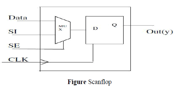
| A.SCAN FLOP |
| The test application time is reduced while preserving the test quality or the fault coverage for circuit testing. The goal is achieved by reducing the number of scan flip-flops required for a scan-based design, and the basic procedure is to look for groups of "s-independent inputs." The s-independent inputs in a group have the property that, when these inputs are combined together to share a scan flip-flop, the originally detectable faults are still detectable under the new scan structure. Though the number of test vectors may slightly increase, this can be offset by the significant reduction in the scan test width. Thus, the goal of test time reduction for scan test can be accomplished. For circuits which have few sindependent inputs, bypass storage cells are added to increase the s-independencies among all inputs. Experiments have been performed on MCNC benchmarks and the results are good. Several benchmark circuits have shown more than 90% of test time reduction. |
 |
| Power consumption in scan-based testing is a major concern nowadays. In this paper, we present a new X-filling technique to reduce both shift power and capture power during scan tests, namely LSC-filling. The basic idea is to use as few as possible X-bits to keep the capture power under the peak power limit of the circuit under test (CUT), while using the remaining X-bits to reduce the shift power to cut down the CUT’s average power consumption during scan tests as much as possible. In addition, by carefully selecting the X-filling order, our X-filling technique is able to achieve lower capture power when compared to existing methods. Experimental results on ISCAS’89 benchmark circuits show the effectiveness of the proposed methodology. |
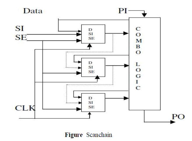
| B.SCAN CHAIN |
| Rapid and reliable test of SOCs necessitates upfront consideration of the test power issues. Special attention should be paid to scan based cores as the test power problem is more severe due to excessive switching activity stemming from scan chain transitions during shift operations. We propose a scan chain modification methodology that transforms the stimuli to be inserted to the scan chain through logic gate insertion between scan cells, reducing scan chain transitions. We provide a mathematical analysis that helps model the impact of scan chain modifications on test stimuli transformations. Based on this analysis, we develop algorithms for transforming a set of test vectors into power-optimal test stimuli through cost-effective scan chain modifications. Even in the highly challenging case of fully specified test vectors, more than an order of magnitude reduction in scan-in power is attained by the proposed methodology, exceeding previous power reduction levels significantly. |
| Functional scan chains are scan chains that have scan paths through a circuit’s functional logic and flip-flops. Establishing functional scan paths by test point insertion (TPI) has been shown to be an effective technique to reduce the scan overhead. However once the scan chain is allowed to go through functional logic, the traditional alternating test sequence is no longer enough to ensure the correctness of the scan chain. Here the faults that affect the functional scan chain, and show a methodology to find tests for these faults. Our results have the number of undetected faults at only 0.006% of the total number of faults, or 0.022% of the faults affecting the scan chain. |
 |
| There are two types of test power: average test power and peak test power. The former is the ratio between the total energy consumed during test and the test time, while the latter is the maximum power consumed during test. High average test power leads to high heat dissipation, which is the cause of chip or package damage as well as reliability degradation due to hot spots . This is especially a serious problem for low-power devices, which usually have low heat dissipation limits. On the other hand, high peak test power may cause excessive circuit noise and result in false failures during test. This is intolerable since it lowers the manufacturing yield of low power devices, pushing up their costs. |
IV.PROPOSED METHOD COMPARE WITH EXISTING METHOD |
| The power consumption of IC during test mode is higher than its normal mode. This brings the power as one of the major design constraints for today’s low power design technologies. In normal scan based test circuits most of the power consumed due to the switching activity of scanflops during shift and capture cycles. Here a novel scanflop is presented which reduces the switching activity of the scanflop for clock and it reduces the power consumption of the circuit and it also reduces area and test time too. The proposed Dual Mode One Latch Double Edge Triggered (DMOL DET) scanflop which shift the two bits of test vector in a clock cycle, during its test mode and captures the single data in a clock cycle during its data mode. The design and functionality of the proposed scanflop is discussed and compared with the different flipflops which shows that the proposed scan flop reduces the test time and clock switching activity by 50%, area by 30% and static power by 25%. |
| In proposed method the power and area consumption were reduced compared with the existing method. Because in this method we used gates and comparators instead of flip flops and transistors. |
V.RESULT ANALYSIS |
| A.FOR EXISTING METHOD |
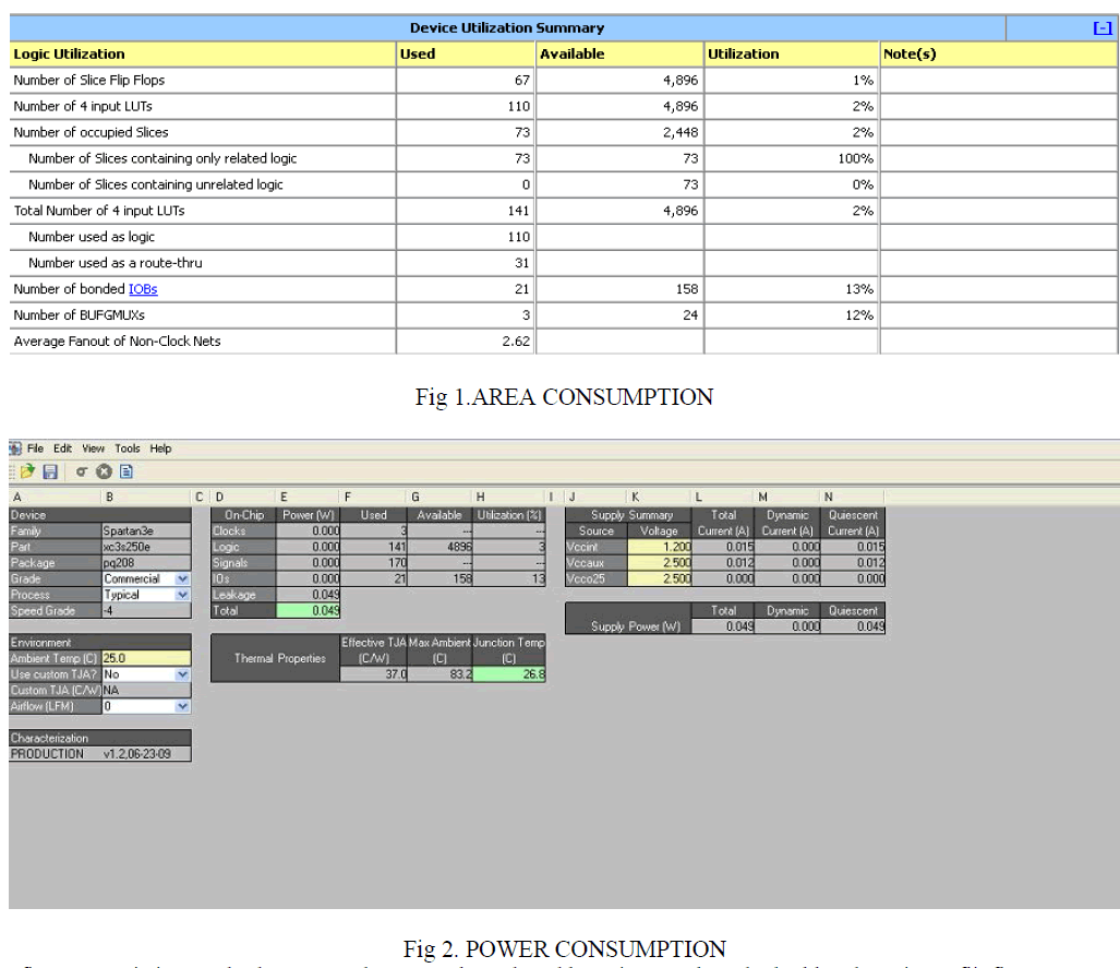 |
| In fig 1&2, Existing method power and area can be reduced by using Dual mode double edge trigger flipflop |
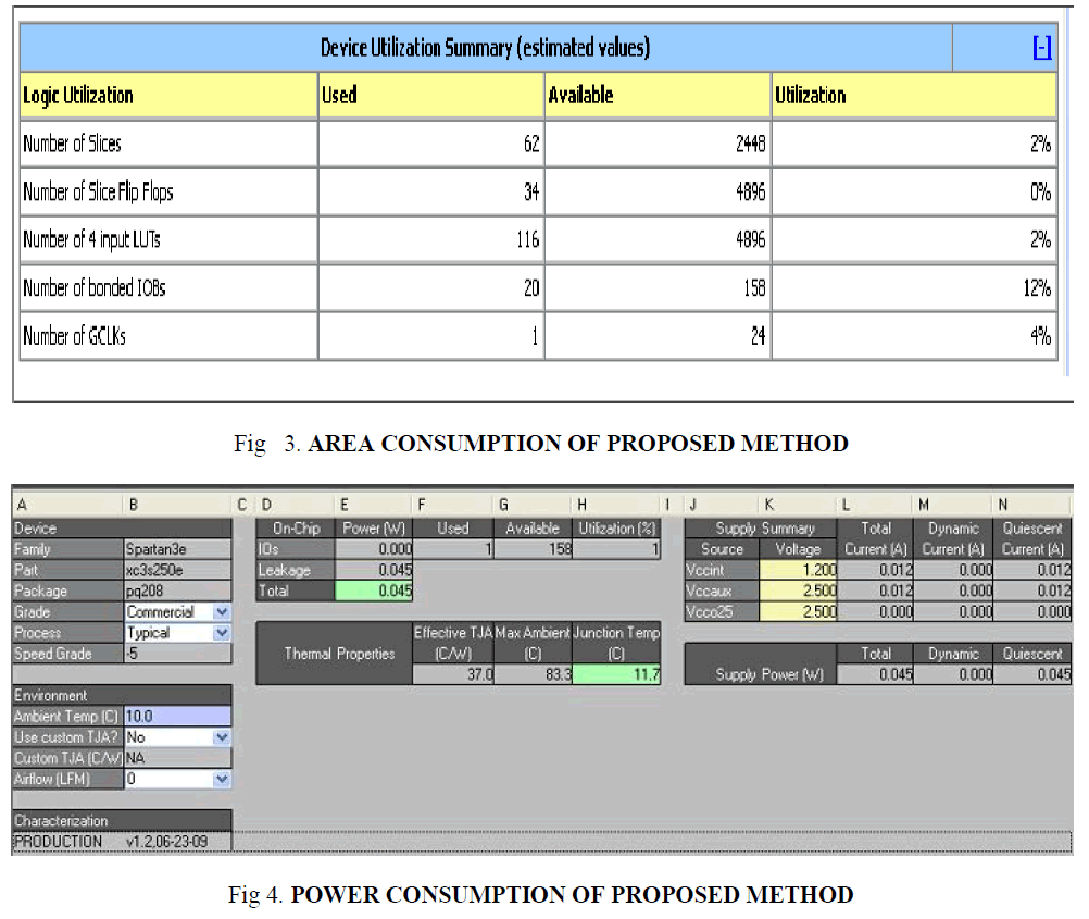 |
| In fig 3 &4 proposed method power can be reduced 25% and area can be reduced 35% by using Dual mode double edge trigger flipflop and the speed of testing get increased during shift cycle for about 50% when compared to the usual scanflop. |
VI.CONCLUSION |
| It is observed from the result that DMOL-DET reduces the chip area about 30% when compared to the ordinary scanflop and 43% when compare to the Pipelined DET scanflop. It also reduces the static power about 25% when compared to the usual scanflop, 35% when compared to the pipelined DET scanflop and the speed of testing get increased during shift cycle for about 50% when compared to the usual scanflop. As a conclusion the DMOL-DET can be used in the digital circuit as a good scanflop for testing purpose which helps in reducing the area, power and increasing speed. In proposed method, precomputation, and gated logic are the two techniques which are used in the scanflops to effectively reduce the power. |
References |
|