Keywords
|
| Leakage power, clock gating, multi mode power switches, power consumption reduction, reconfigurable power-gating structure. |
INTRODUCTION
|
| As chip density increases persistently along Moore’s law, power consumption is emerging as a major trouble for contemporary systems. Dynamic power is tackled nowadays by the reduction of the supply voltage level. Dynamic energy is proportional to the square of the supply voltage. Thus, a lower voltage level yields a quadratic reduction in the energy consumption. To further reduce the dynamic power, systems-on-chip (SoCs) are partitioned into voltage islands with separate supply rail and unique power characteristics. Separate power management policies (such as dynamic supply voltage scaling) can be applied in each region, thereby further reducing dynamic power. The reduction of the power supply voltage level adversely affects the execution time. In order to maintain system performance, the transistor threshold voltage (Vt ) is reduced. The reduction of the threshold voltage however adversely affects the subthreshold leakage current, which increases exponentially. Moreover, as devices keep shrinking, the channel length shortens and the gate oxide thickness reduces, increasing the gate-induced drain leakage, the gate oxide tunneling current, and the junction leakage. For technologies below 90 nm, leakage (static) power is so high that it is comparable in magnitude to dynamic power consumption. |
RELATED WORK
|
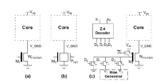
| The classical power switch architecture is shown in Fig. 1(a). It consists of a high-Vt footer transistor MP connected between the core and the ground rail (the bold line on the gate indicates a high-Vt transistor). When the footer is “on,” the core operates in the normal functional mode. When it is “off” (i.e., during idle mode), the virtual ground rail (V_GND) charges to a voltage level close to the power supply and it suppresses the leakage power of the transistors of the circuit. In order to minimize the impact on circuit performance during normal operation, the footer transistor is made large enough and constitutes a strong driver. In practice, instead of using a large footer transistor (macro-switch), many small transistors (micro-switches) connected in parallel are used. In order to restore the virtual ground rail to its nominal value when the circuit transitions from the power-off mode to the active mode, the parasitic capacitance at the V_GND node has to be completely discharged through the power switches. However, the aggregate size of the power switches is not very large due to area constraints, while at the same time power switches are made of low-performing high-Vt transistors in order to minimize the leakage current. As a result, the wakeup time is usually long relative to the circuit clock rate. This limits the applicability of this technique to idle periods that are longer than the wake-up time of the circuit. Consequently, the full leakage-savings potential of this architecture is not fully exploited. To overcome this limitation, proposed the use of an intermediate power-off mode, where the virtual ground node is left charged to an intermediate voltage level. This is achieved through the use of a pMOS device connected in parallel with the nMOS footer MP , as shown in Fig. 1(b). The pMOS is turned on in the intermediate power-off mode, and the virtual ground potential is adjusted to the threshold voltage of the pMOS. Then the virtual ground node requires less time to discharge, although at the expense of less leakage reduction compared to the complete power-off mode. |
| A power-switch structure with two intermediate power off modes is presented in Fig. 1(c). It consists of the power switch MP , a decoder, the bias generator, which is an analog circuit, and the transistors T0−T3. Using this structure, the gate voltage of the power switch MP is regulated to four different voltage levels 0, V1, V2, and Vdd, which correspond to three power modes, namely Snore, Dream, Sleep, and Active, respectively. Transistor T0 adjusts the gate voltage of MP at the ground level, and thus it completely turns off the power switch. This is the Snore mode where the leakage power is minimized and the wake up time is very high (MP has to discharge the virtual ground rail from nearly Vdd to ground when it is turned on). The next two modes, namely Dream and Sleep, are determined by the two subthreshold gate voltages V1, V2, (V1 < V2 < VTH−SW, where VTH−SW is the threshold voltage of the power switch transistor MP ) generated by the bias generator and applied to the gate of the power switch through transistors T1, T2, respectively. In both cases, the virtual ground is charged to a potential that is lower than Vdd and thus the wake-up time drops. However, the leakage power consumed increases compared to the Snore mode, but it is still much lower than the leakage current of the Active mode. By turning on transistor T3, the gate voltage level is set to Vdd and the core is put into Active mode. |
PROPOSED ARCHITECTURE
|
MULTI-MODE POWER-GATING ARCHITECTURE
|
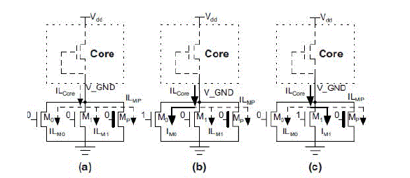
| It consists of the main power switch transistor MP and two small transistors M0 and M1, each corresponding to an intermediate power-off mode (M0 corresponds to the dream mode and M1 corresponds to the sleep mode). Transistor MP is a high-Vt transistor and it remains on only during the active mode. Transistors M0 and M1 are small low-Vt transistors that are turned on only during the corresponding power-off mode. The various modes of operation are as follows. |
| Active Mode: The Transistors MP, M0, M1 are on. |
| Snore Mode: Transistors MP , M0, and M1 are off as shown in Fig. 2(a). In this case, the leakage current of the core, I Lcore, is equal to the aggregate leakage current flowing through transistors M0, M1, MP (I Lcore = I LM0 + I LM1 + ILMP), which is very small.Thus the voltage level at V_GND is close to Vdd and the circuit consumes a negligible amount of energy, but the wake-up time is high. |
| Dream Mode: Transistor M0 is on and transistors MP and M1 are off as shown in Fig. 2(b). The current flowing through transistor M0 (and thus the aggregate current flowing through M0, M1, and MP) increases because M0 is on (IM0 > I LM0). The exact value of IM0 depends on the size of transistor M0, and it sets the virtual ground node at a voltage level which is lower than Vdd (i.e., VV_GND < Vdd). Thus the static power consumed by the core is higher compared to the snore mode and the wake-up time is less. |
| Sleep Mode: Transistor M1 is on, and MP, M0 are off as shown in Fig. 2(c). The transistor M1 has larger aspect ratio than M0 (WM1/LM1 > WM0/LM0), the aggregate current flowing through M0, M1, and MP increases even more when M1 is on (note that IM1 > IM0). Consequently, the voltage level at the virtual ground node is further reduced compared to the dream mode and thus the wake-up time decreases at the expense of increased power consumption. |
RECONFIGURABLE ARCHITECTURE
|
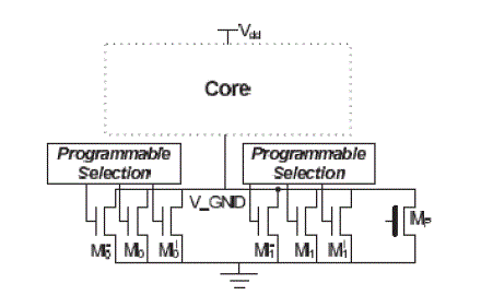
| The proposed architecture exhibits considerable tolerance to process variations. However, for cases where even higher tolerance to process variations is required, we propose the reconfigurable structure shown in Fig. 3. Each of the M0, M1 transistors is replaced by a triplet of transistors (M−0,M0, M+0 ), (M−1 , M1, M+1), respectively. The aspect ratios of M0 and M1 are calculated analytically as in the previous subsection. The aspect ratios of (M−0 ,M+0),(M−1,M+1) are selected to be close to the aspect ratio of M0, M1, respectively. |
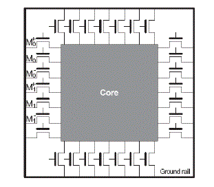
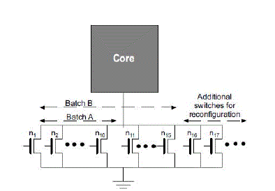
| The reconfigurable architecture has low cost due to its simplicity and the small size of transistors M0, M1. For even higher tolerance to process variations, the reconfigurable structure can be easily extended to accommodate groups of more than three transistors per mode. The n pairs of transistors with their aspect ratios shifted by α1%, α2%, . . . ,αn% above and below the nominal value of the aspect ratio will be used in each group (α1 < α2 < · · · < αn). The cost of the reconfigurable structure can be further reduced if we exploit the similarity of this structure to the architecture of the main power switches. As shown in Fig. 4, the main power switch is constructed from many microswitches connected in parallel. We can exploit these transistors (which already exist in the design) to embed the proposed architecture into the main power switch architecture. Specifically, we select an appropriate subset of these microswitches and we size them according to the design method proposed in Section III-B. These switches are indicated in Fig. 4 as M+0 , M0, M−0 , M+1 , M1, M 1 . (Note that more microswitches can be configured accordingly for implementing more power-off modes and/or for offering higher amount of redundancy.) During the active mode of operation, these switches are turned on, similar to the rest of the microswitches (i.e., they play the role of the main power switch at this mode). However, during the power-off mode they are controlled separately from the rest of the switches and they are separately turned-off or turned-on based on the programmable selection and the power-off mode applied. Using this technique, no additional power switches are needed for implementing the reconfigurable architecture and thus its cost is considerably reduced. |
| For example, in Fig. 5 we present one such case where the design method yielded the following results: WM0 = 10 × Wmin and WM1 = 15 × Wmin. Note that Wmin is the minimum width allowed in the technology and also LM0 = LM1 = Lmin. Each of the n1, n2, n3, . . . transistors has minimum size Wmin, Lmin. By turning on all the 10 transistors n1, n2, . . . , n10 of batch A during the power off mode, we implement a similar functionality to turning on power switch M0 (the aggregate width of n1, . . . , n10 is equal to the width of transistor M0). By turning on all the 15 transistors n1, n2, . . . , n15 of batch B, we implement a similar functionality to turning on power switch M1 (their aggregate width is equal to the width of transistor M1). The reconfigurability of this structure is provided by adding more transistors in parallel (n16, n17, . . .) as well as by adjusting the number of transistors participating in each batch A, B. For example, in the case of M0, the value of α = ±10% means that one additional or one less transistor ni should be turned on during the power off mode i.e., batch A consists of either 9 or 11 transistors (note that W+ M0=WM0+0.1·WM0= 11×Wmin and W−M0= WM0− 0.1·WM0= 9 × Wmin). The same can be done for batch B. This is an alternative way to shift the width of the M0 and M1 transistors by ±α%. |
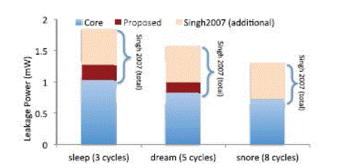
| The leakage power consumed during the power-off modes by the core and the power-gating logic in the two architectures. The three power-off modes, i.e., sleep, dream, and snore, which require 3, 5, and 8 wake-up cycles and the clock frequency is taken to be 1 GHz. The y-axis shows the leakage power consumed in three parts: i.e., the static power consumed by the core, the static power consumed by the proposed scheme, and the additional static power consumed by the scheme proposed in.The total power consumed by the scheme proposed in is the sum of the two topmost parts of each bar. Both architectures provide a tradeoff between the wake-up time and the static power reduction. However, the proposed scheme is more effective than that in [42] in reducing the total static power for the same number of wake-up cycles. The logic core consumes the same static power at each power-off mode in both schemes because the voltage level at the virtual ground node is the same for both architectures. Specifically, for both schemes the reduction of the static power of the core is equal to 89.9%, 92%, and 92.9% in the sleep, dream, and snore modes, respectively. The difference in static power reported in Fig. 6 at each power-off mode is mainly attributed to the proposed scheme. Note that the bias generator has an always-on path from the power supply to the ground, which consumes increased power even in the snore and active modes where the bias generator is not used. In contrast, transistors M0 and M1 of the proposed scheme consume negligible static power during the snore mode, as shown in the rightmost bar in Fig. 6, as well as during the active mode. |
EXPERIMENTAL RESULTS AND COMPARISON
|
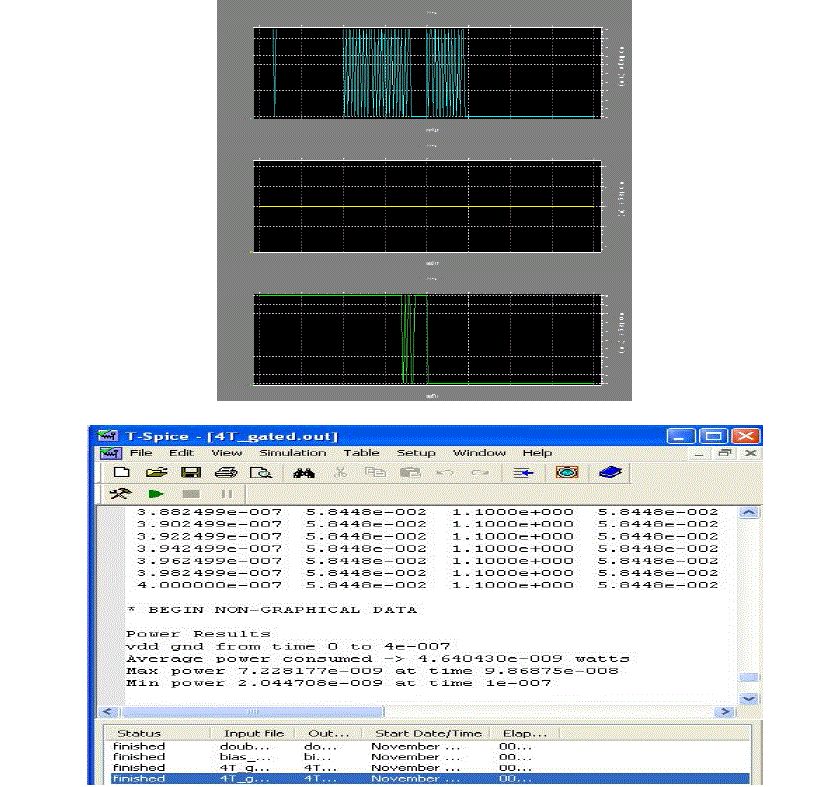
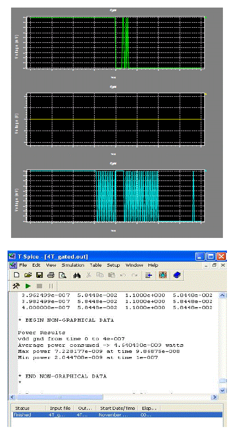
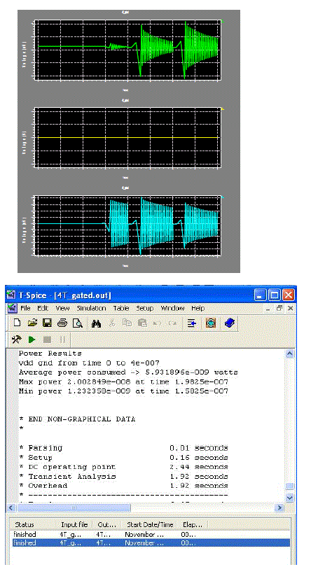
| The experimental results of different modes with power consumption by using simulation software is shown below. The results shows that,the proposed design consumes less power compared to existing technique. |
CONCLUSION
|
| We described a new power-gating scheme that provides multiple power-off modes. The proposed design offered the advantage of simplicity and requires minimum design effort. Extensive simulation results showed that, in contrast to a recent power-gating method, the proposed design is robust to process variations and it is scalable to more than two poweroff modes. Moreover, it requires significantly less area and consumes much less power than the previous design. Finally, a reconfigurable version of this method can be used to increase the manufacturability and robustness of the proposed design in technologies with larger process variations. |
Figures at a glance
|
 |
 |
 |
 |
 |
| Figure 1 |
Figure 2 |
Figure 3 |
Figure 4 |
Figure 5 |
 |
 |
 |
 |
| Figure 6 |
Figure 7 |
Figure 8 |
Figure 9 |
|
References
|
- Static Power Reduction Using Variation-Tolerant and Reconfigurable Multi-Mode Power Switches Zhaobo Zhang, Student Member, IEEE,XrysovalantisKavousianos, Member, IEEE, KrishnenduChakrabarty, Fellow, IEEE, and YiorgosTsiatouhas, Member, IEEE, IEEE transactions on very large scale integration (vlsi) systems, vol. 22, no. 1, january 2014
- D. Lackey, P. Zuchowski, T. Bednar, D. Stout, S. Gould, and J. Cohn, “Managing power and performance for system on-chip designs using voltage islands,” in Proc. IEEE/ACM Int. Conf. Comput. Aided Design , Nov. 2002, pp. 195–202.
- R. Puri, D. Kung, and L. Stok, “Minimizing power with flexible voltage islands,” in Proc. IEEE Int. Symp. Circuits Syst., May 2005, pp. 21–24.
- R. Puri, L. Stok, J. Cohn, D. Kung, D. Pan, D. Sylvester, A. Srivastava, and S. Kulkarni, “Pushing ASIC performance in a power envelope,” in Proc. Design Autom. Conf., Jun. 2003, pp. 788–793.
- K. Roy, S. Mukhopadhyay, and H. MahmoodiMeimand, “Leakage current mechanisms and leakage reduction techniques in deepsubmicrometerCMOS circuits,” Proc. IEEE, vol. 91, no. 2, pp. 305–327, Feb. 2003.
- S. Idgunji, “Case study of a low power MTCMOS based ARM926 SoC: Design, analysis and test challenges,” in Proc. IEEE Int. Test Conf., Oct. 2007, pp. 1–10.
- A. Abdollahi, F. Fallah, and M. Pedram, “Leakage current reduction in CMOS VLSI circuits by input vector control,” IEEE Trans. Very LargeScale Integr. (VLSI) Syst. vol. 12, no. 2, pp. 140–154, Feb. 2004.
- Y. Alkabani, T. Massey, F. Koushanfar, and M. Potkonjak, “Input vector control for post-silicon leakage current minimization in the presence of manufacturing variability,” in Proc. 45th ACM/IEEE Design Autom. Conf., Jun. 2008, pp. 606–609.
- K. Kim, Y.-B. Kim, M. Choi , and N. Park , “Leakage minimization technique for nanoscale CMOS VLSI,” IEEE Des. Test Comput., vol. 24, no. 4, pp. 322–330, Jul. 2007.
|