International Journal of Advanced Research in Electrical, Electronics and Instrumentation Engineering
ISSN ONLINE(2278-8875) PRINT (2320-3765)
ISSN ONLINE(2278-8875) PRINT (2320-3765)
Nithin George1, Elizabeth Sebastian2, Reenu George3
|
| Related article at Pubmed, Scholar Google |
Visit for more related articles at International Journal of Advanced Research in Electrical, Electronics and Instrumentation Engineering
The practical performance evaluation of a full-bridge phase-shift-modulated DC-DC converter is presented in this paper. The converter has the property of zero voltage switching (ZVS) using the transformer leakage inductance, without the need for any additional components. The implementation aspects of the converter are discussed, including the design of the high frequency transformer and LC filter, and configuration of the signal generation system and the driving circuits. The experimental results from a 450 W prototype are provided and these support the case for ZVS taking place in the converter. The effectiveness of the design is validated by the full load efficiency of 92% that was given by the prototype
Keywords |
| Full-bridge DC-DC converter, zero voltage switching, phase-shift-modulation, practical evaluation. |
INTRODUCTION |
| A DC-DC converter forms the main part of a Switch Mode Power Supply (SMPS), fuel cell power conditioning unit, battery charger, etc. Such a DC-DC converter may be of isolated or non isolated type. Isolated DC-DC converters can employ topologies including forward, flyback, push-pull, half-bridge and full-bridge [1]. Of the different topologies available, the full-bridge converter is quite popular due to its symmetric mode of operation and large power handling capability. |
| For full-bridge DC-DC converter different switching techniques are available; of these, the Phase Shift Modulation (PSM) technique is widely used. The main reason for this is the soft switching i.e., Zero Voltage Switching (ZVS) that is offered by the PSM technique. No extra components are needed and the circuit parasitics: the device capacitance and transformer leakage inductance are used for attaining ZVS. PSM technique and the design considerations were first detailed in [2]. |
| This paper discusses various aspects associated with design and implementation of a PSM full-bridge DC-DC converter having a full load capacity of about 450W. The converter uses a high step ratio of 1: 6 and such ratios are widely seen in fuel cell power conditioning systems [3]. The design aspects of the transformer and the LC filter at the output are discussed in detail. Also the implementation aspects like generation of signals, isolation between the HV and LV circuits, and driving requirements are given a brief look-through. Through the experimental results, the evidence for ZVS is presented |
THE CONVERTER |
| The full-bridge DC-DC converter is sketched in Fig. 1(a). In PSM technique, the two legs of the active bridge are operated with a phase shift po as shown in Fig. 1(b). The phase shift angle and duty cycle of the converter are related by: |
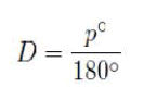 |
| The phase shift operation results in the discharge of the switch output capacitance and forcing of the anti parallel diode of the switch into conduction even before the switch itself starts to conduct. Thus the switch is turned on at zero voltage. |
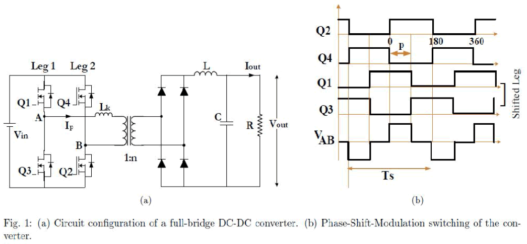 |
| The energy stored in leakage inductance Lk is used to discharge the device output capacitances and force conduction of the body diodes of Q2 and Q4. If the load current is small, the energy stored may not be enough for this process and ZVS may not take place. The critical value of load current below which ZVS is lost is found to be inversely proportional to the magnitude of Lk [2]. In the case of devices Q3 and Q1, the energy stored in the filter inductance L is also available, in addition to that stored in Lk, to discharge the output capacitances and force conduction of the diodes. Thus even for light loads ZVS can be achieved for these two devices. |
| In PSM switching of the converter, the duty cycle of the voltage at the secondary is found to be smaller than that of the primary. This is due to the finite slope associated with the rise and fall of transformer primary current Ip. The effective duty cycle De (or duty cycle at secondary) is given as [4]: |
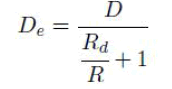 |
| where Rd = 4 n2 Lk fs. fs indicates the switching frequency, and R the load resistance. From (2) it can be inferred that a higher value of Lk results in a lower De. Thus the choice for Lk is influenced by conflicting factors: ZVS and gain reduction. |
| Finally, the relationship between Vin and Vout will have to be defined: |
| which is similar to that of a buck/forward converter. |
IMPLEMENTATION AND DESIGN ASPECTS |
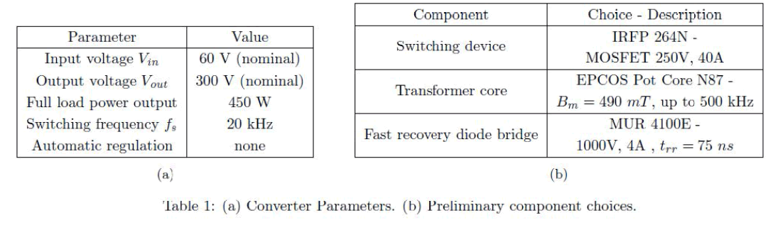
| It is intended to develop a DC-DC full bridge converter with the specifications as given in Table 1(a). Based on the above requirements the preliminary component choices are made and they are listed in Table 1( b). |
A. Transformer |
| Once a core material is chosen, the turns ratio 1: n and the number of turns in the primary and secondary windings will have to be determined. The value of n can be found out using the relationship: |
 |
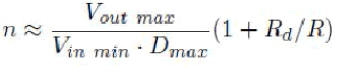 |
| Since Vout is to be 300 V, n = 6 is chosen. This will ensure the nominal output voltage even at a reduced Vin of about 55 V. |
| The rms value of induced emf in the transformer primary winding can be written as: |
| where Bm is the maximum flux density permissible in the core, Ai the iron area and Np the number of turns in the primary. This equation is based on operation of the transformer with a sinusoidal supply. The transformer in the instant case is subjected to quasi square wave VAB as shown in Fig. 1(b) and the rms value of fundamental component of this waveform is given by [5]: |
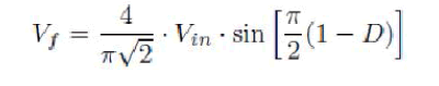 |
| The design of the transformer is based on the assumption that it is subjected to this fundamental component of voltage Vf. For Vin = 60 V and duty cycle D=1, the value would be obtained as Ep =Vf = 54 V from (6). Now a core size 62/49, which has an iron area Ai of 570 sq. Mm, is chosen [6]. This is a preliminary choice, later on if this core is found not to have suitable window area to accommodate the windings, the next higher core size may be chosen |
| Further, the B-H curve of the transformer core material has to be looked into, and avoiding the saturation region, a maximum flux density Bm of 100 mT is chosen for operation. Substituting for all the known values in (5), Np may be chosen as 13. Also the number of turns in the secondary, Ns may be determined as 78 without any doubt. |
| With regard to the gauge chosen for the windings, the primary and secondary currents at full loads may be determined, and gauge of wires chosen from a gauge table [7]. A check is performed to ensure that the windings would be accommodated in the window area of the pot core and for this the following relation may be used: |
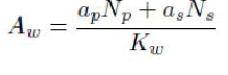 |
| where ap, as is the cross sectional area of the 1o and 2o winding wires respectively and Kw is the window factor, a value lying between 0.6 and 0.4. ap and as may be obtained from the gauge tables itself and a substitution in the above relationship gives the window area Aw. If the window area calculated is more than the actual window area, the next higher core size will have to be chosen and design repeated. If the calculated window area is less, either this design may be adopted or a redesign may be made with a smaller core size. |
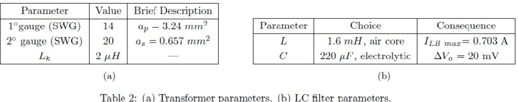
| Once the transformer is wound, immediately the leakage inductance is determined by conducting short circuit test using an LCR meter. The parameters of the transformer are summarized in Table. 2( a). |
 |
B. LC Filter |
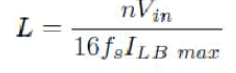
| Once the transformer is designed, the next significant design is associated with the 2nd order LC filter at the output. The value of inductance L determines the boundary of discontinuous conduction mode. If the value of inductance is large, the current value which forms the boundary between continuous and discontinuous conduction mode will be smaller, ie., continuous conduction mode can be assured for smaller values of load currents [5]. The relationship between the L and the maximum value of boundary load current is given by: |
 |
| Usually converters are operated in continuous conduction mode and the expression (2) is only valid during this mode. Also the small signal model during the two modes is quite different. |
| Capacitor value is chosen based on the maximum output voltage ripple that can be tolerated. The expression for maximum peak to peak output voltage ripple is given by: |
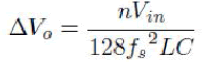 |
| Now based on the requirements, values are chosen for L and C, and the choices with their consequences are listed in Table. 2(b). |
C. Gating Signal Generation |
| A 16 bit PIC microcontroller, dsPIC30F2010, is used to generate the four gating signals for the switches. This PIC has an inbuilt PWM module and using this in conjunction with an infinite loop algorithm, the PSM signals are generated. |
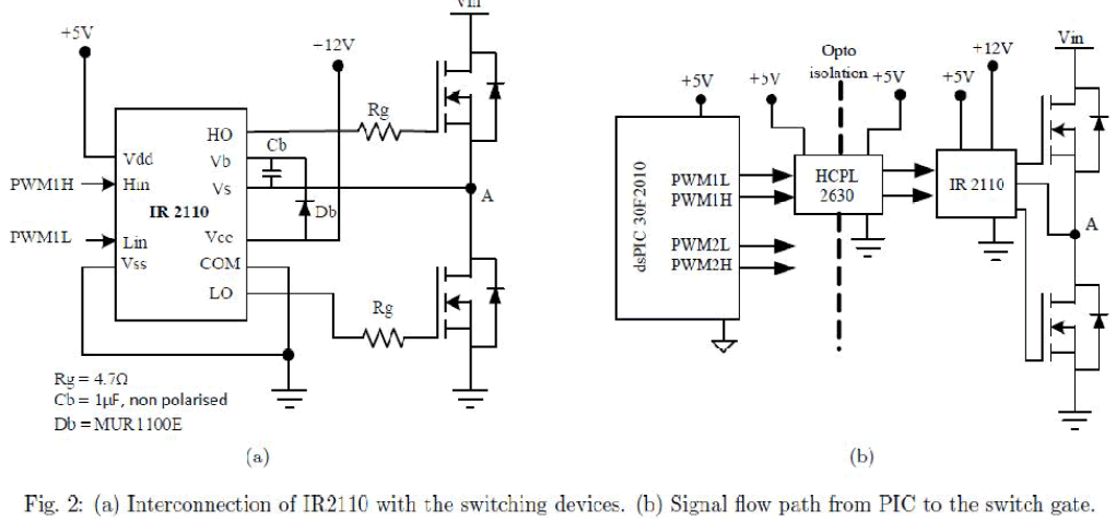
| In order to prevent any chance of unreliable operation of the microcontroller, the ground of the 5 V supply given to the PIC is kept isolated from the supply ground of the driver and DC rail. For transmission of signals from one circuit to another, an optocoupler is used. HCPL 2630 is the IC used for this purpose in the instant case, and it can handle two channels per IC. |
D. Driving |
| Considering a single leg of the full bridge DC-DC converter, while the lower device can be driven by any source as long as it can supply the required current, the upper device cannot be driven so due the floating nature of its source. Thus in order to drive it a driver IC is required. IR2110 is one such IC that can be used to drive both the devices in a single leg. For the upper device it employs a bootstrap mechanism and the gate voltage of the device would be 15-12 V higher than the DC rail voltage Vin. It may be noted that the ground of driver IC is made common with the DC rail. The connection of the IR2110 IC with the switching devices is illustrated in Fig. 2(a), while Fig. 2(b) shows the signal flow path from the microcontroller to the device gate. |
EXPERIMENTAL RESULTS |
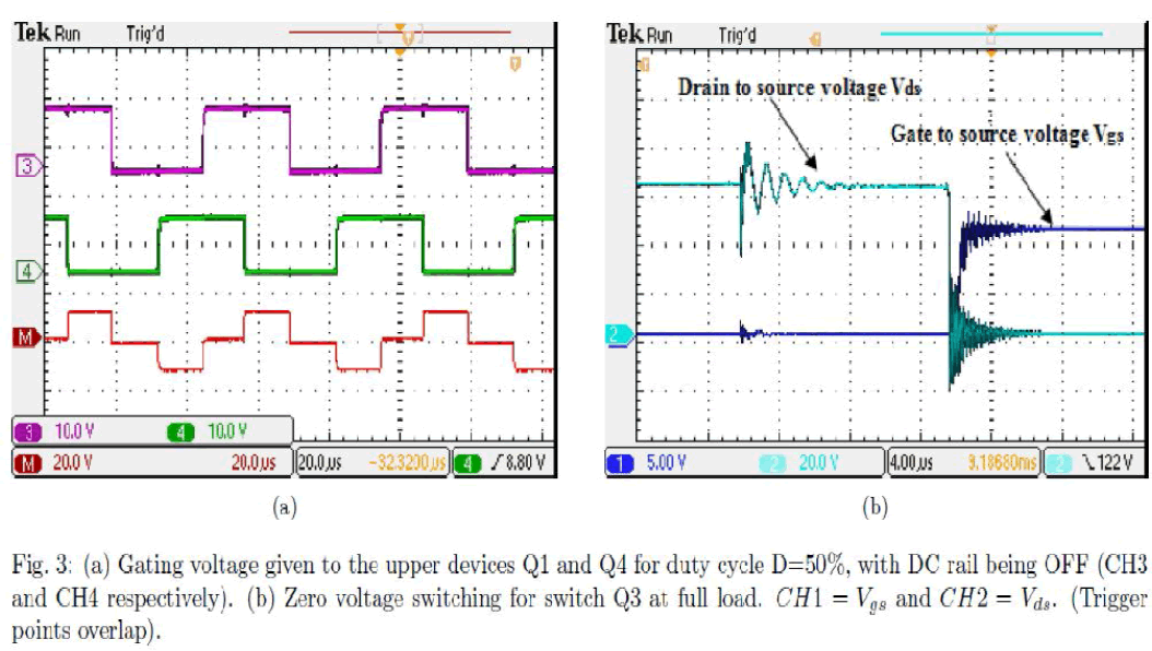
| Fig. 3(a) shows the driving signals given to the upper devices Q4 and Q1. The waveforms were taken with the DC rail OFF, limiting the amplitude of the driving voltages to 12 V. Math shows CH3-CH4 and are a scaled version of transformer primary voltage VAB. The evidence for ZVS in a switch is obtained by observing its gate voltage together with the drain-to-source voltage Vds. ZVS is obtained at turn ON and if Vds goes low even before the gate-to-source voltage Vgs goes high, it |
 |
| indicates conduction of diodes and hence ZVS. The waveforms in relation to this for Q3 at full load condition are shown in Fig. 3(b) and ZVS can be observed clearly. |
 |
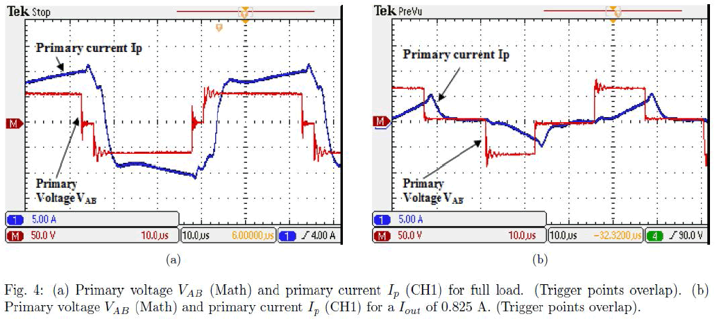
| The primary voltage VAB waveform, determined by subtracting VB from VA, is shown in Fig. 4. The primary current Ip waveform is also shown. The waveforms in Fig. 4(a) are for Vout = 299 V and R = 200 ohms ie., full load. The waveforms may be compared to the theoretical prediction in [2] and the similarity noted. The conduction of diodes prior to conduction of devices is clear and yet another evidence of ZVS is obtained. Fig. 4(b) shows the same waveforms for a duty cycle of 50 % and Iout of 0.825 A, with R=200 ohms. Lack of ZVS is clear from the waveforms. |
 |
| The filtered output voltage together with the current drawn from the input DC supply is shown in Fig. 5(a). The waveform is taken at D=90 %, Vout =299 V and R = 200 ohms. The efficiency curve of the converter is shown in Fig. 5(b). It can be seen that beyond 300 W the curve is almost a constant at 92 %, showing the ideal loading region for the present converter design. |
CONCLUSION |
| This paper has demonstrated design, implementation and practical evaluation of a zero voltage switching, phase-shiftmodulated, full-bridge DC-DC converter. The implementation aspects have been elaborated in detail with special emphasis being given to high frequency transformer design. The driver circuitry together with the signal generation mechanism has been given a detailed look-through. The signal flow path through the optocoupler and its need has also found a mention in the paper. |
| Since practical evaluation was the main objective, a significant amount of results in this regard has been presented. Two evidences for ZVS in the converter switches have been obtained from the experimental study. The efficiency curve of the converter shows a maximum efficiency of 92 % at full load, indirectly supporting the case for ZVS. |
References |
|