International Journal of Advanced Research in Electrical, Electronics and Instrumentation Engineering
ISSN ONLINE(2278-8875) PRINT (2320-3765)
ISSN ONLINE(2278-8875) PRINT (2320-3765)
| V.M. Ramaa Priyaa Assistant professor, Dept. of E&I, Bharath University, Chennai, India |
| Related article at Pubmed, Scholar Google |
Visit for more related articles at International Journal of Advanced Research in Electrical, Electronics and Instrumentation Engineering
Predictive control is a very wide class of controllers that have found rather recent application in the control of power converters. Research on this topic has been increased in the last years due to the possibilities of today’s microprocessors used for the control. This paper presents the application of different pre-dictive control methods to power electronics and drives. A simple classification of the most important types of predictive control is introduced, and each one of them is explained including some application examples. Predictive control presents several advan-tages that make it suitable for the control of power converters and drives. The different control schemes and applications presented in this paper illustrate the effectiveness and flexibility of predictive control
Keywords |
| Drives, power electronics, predictive control. |
INTRODUCTION |
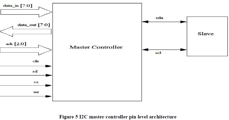
| The design of I2C bus controller will be interface to integrate for the purpose to communicate between them i.e. the onchip RAM (EEPROM), Oscillator (RTC), ADC. The presence of a RTC and an on chip RAM support for a data communication between the chip and a host computer to send data on the RAM. To minimize the system-level interconnect between integrated devices, I propose to transmit the contents of the RAM storing the results back to a host computer via a serial bus, the I2C Interface. The interconnect integrated circuit bus commonly known as the I2C bus which is a bi-directional, two-wire and serial communication standard protocol. The designed are simple but difficult for efficient integrated circuit (IC) control. The system is comprised of two bus lines, SCL (Serial Clock) and SDA (Serial Data). Each device can be identified by a unique 7 or 10 bits-address. The I2C protocol supports to multiple master but this application discusses only a Master and a Slave system implementation. Standard I2C devices operate up to 100Kbps, while fast-mode devices operate at up to 400Kbps. Most of the I2C devices available today support 400Kbps operation. |
BUS SPECIFICATIONS OF I2C |
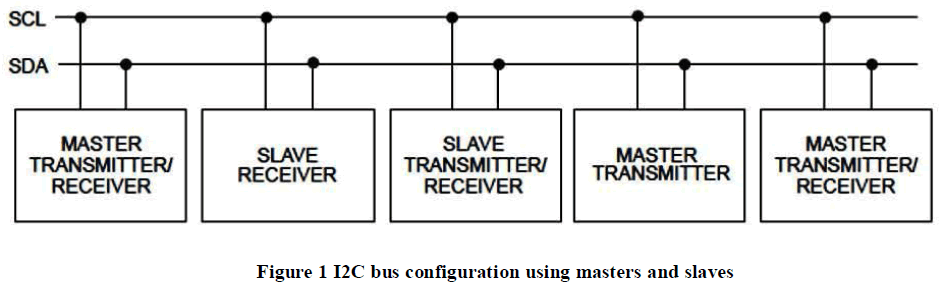
| The Philips semiconductor was introduced by I2C standard protocol for communicate with faster to various slower devices and communicate with each other, without data loss. The I2C bus component are used, a bi-directional two wire. First is SDA(serial data) and second is SCL(serial clock). I2C-bus supports any IC fabrication process i.e. it may be NMOS or CMOS or bipolar. Each device recognized by a unique 7 or 10 bit address ( microcontroller, LCD driver, EEPROM, ADC or RTC). Its can operate as either a transmitter or receiver, depending on the function of the device. Obviously an LCD driver is only a receiver whereas a memory can both receive and transmit data. In addition to transmitters and receivers, devices can also be considered as masters or slaves when performing data transfers. |
I2C Bus Terminology: |
| Transmitter: The device which sends the data or message to the receiver. |
| Receiver: The device which receives the data or message from the bus. |
| Master:-The device which generates clock signals, initiates a transfer i.e. start condition and terminates a transfer i.e. stop condition. It may also act as a transmitter/receiver. |
| Slave:-The device addressed by a master. Also it may act as a transmitter/receiver. |
| Multi master: More than one master can attempt control the bus at the same time without demeaning the data/message. |
| Arbitration: It is a procedure to ensure that, if more than one master simultaneously tries to control the bus, only one is allowed to do so and the data is not corrupted. |
| Synchronization: It is a procedure to synchronize the clock signals of two or more devices. |
 |
I2C BUS CONTROLLER DESIGN |
| The design of the master controller for I2C bus is following some step:- |
| (a) START and STOP condition: all transactions begin form START(S) and can be terminated by a STOP (P). A HIGH to LOW transition on the SDA line while SCL is HIGH defines a START condition. A LOW to HIGH transition on the SDA line while SCL is HIGH defines a STOP condition. |
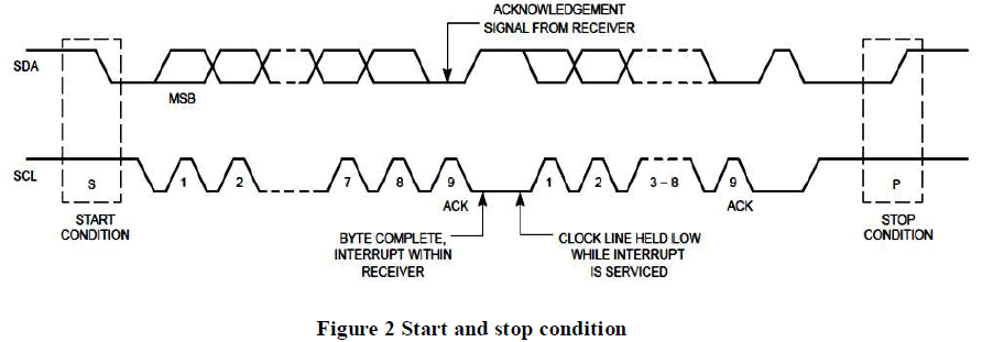 |
| (b) Byte format Data Transfer: every byte must be 8 bit long put on the SDA line. Each byte followed by Acknowledge bit. Which show in figure 2. |
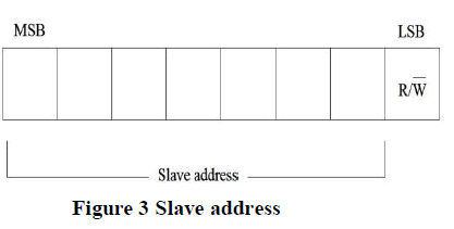
| (c) Device Addressing: the device addressing of the I2C bus are using 8 bit word within one W/R bit which depend on the clock like as if clock is low then write and high then read. |
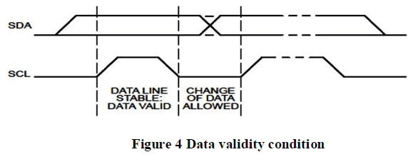
| (d) Data Validity: The data on the SDA line are valid for during high period of clock pulse. |
 |
 |
I2C BUS ARCHITECTURE |
| The I2C bus architecture consists of Master and Slave and there is only one master. The master controller for I2C bus is design on the verilog Hardware Description Language (HDL). I2C is a two-wire, bi-directional serial bus that provides a simple and efficient method of data exchange between devices. |
 |
I2C PROTOCOL AND DESIGN STEP |
| Normally, a standard communication protocol consists of four parts: (a) START signal generation,(b) Slave address transfer,(c) Data transfer,(d) STOP signal generation. |
| The functional description of I2C master has to be described in the Verilog HDL. That is called design module / core. The test bench program has to be developed to test the design module. The test bench gives the input to the design module & verifies the outputs. The test bench has to be written in such way to check the design module in all possible conditions. Verilog simulator tool is used to verify the design functioning (Simulation). |
CONCLUSION |
| We can be interface of between two or more device using a I2C bus and data are serially communicate. Two device as microcontroller (master) and EEPROM (slave) using a I2C bus can be interface of each other. The master controller is design on the verilog HDL, simplifies the design process. It is similar to device address and a unique bits-address on the master and slave device which each device can be identified. The design of master controller is easy but slave design is difficult. The designer can write his design description without choosing any specific fabrication technology. If a new technology emerges, designers do not need to redesign the circuit. He simply input the design program to the logic synthesis tool and creates a new gate level netlist using the new fabrication technology. The logic synthesis tool will optimize the circuit in area and timing for the new technology. |
ACKNOWLEDGMENT |
| The correspondence author is thankful to all the faculty members of department of Electronics & Communication, IES College of Technology Bhopal, M.P. and India for continuous support and encouragement. This is an opportunity to prove our technical skill for the benefit of social civilization. |
References |
|