International Journal of Advanced Research in Electrical, Electronics and Instrumentation Engineering
ISSN ONLINE(2278-8875) PRINT (2320-3765)
ISSN ONLINE(2278-8875) PRINT (2320-3765)
Akhiljith P.J1, Leena Thomas2 and Ninu Joy3
|
| Related article at Pubmed, Scholar Google |
Visit for more related articles at International Journal of Advanced Research in Electrical, Electronics and Instrumentation Engineering
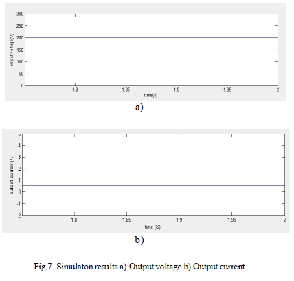
An integrated double buck–boost(IDBB) converter is proposed as a high-power-factor offline power supply for power-LED lamps. The IDBB converter features just one controlled switch and two inductors and is able to supply a solid-state lamp from the mains, providing high power factor and good efficiency. The IDBB converter is analyzed, and a design methodology is proposed. It is demonstrated that, with a careful design of the converter, the filter capacitances can be made small enough so that film capacitors may be used. In this way, the converter mean time between failures can be made as high as that of the solid-state lamp. PWM switching is used for controlling the switching pulses. Feedback circuit is provided with PI controller for accurate result. The converter is simulated using MATLAB 2010 and waveforms are analysed. Simulation results demonstrate that the output voltage of the desired converter can be stably maintained at 200 V and power factor can be improved upto 0.90.
Keywords |
| Continuous Conduction Mode (CCM), Discontinuous Conduction Mode (DCM), Duty cycle (D), Integrated double Buck–boost (IDBB), white power LED |
INTRODUCTION |
| LED lighting is one of the most promising solutions to deal with the increasing energy demands. As natural resources around the world are becoming more expensive and less viable to sustain the needs of increasing populations around the world. Since the encapsulation technology of LEDs has become mature in the recent years, the LEDs are applied to the lighting areas such as the LCD backlight, the street lighting and the car head lightings. Generally, the use of LEDs is in the development direction of the future lighting system. LEDs can be divided into three categories: indicative LEDs, high-brightness LEDs, and power LEDs. Of these White power LEDs are becoming an attractive light source, owing to their high reliability, long life, high color rendering index, and small size [1]. In addition, there are commercially available units that can reach light efficacies as high as100 lm/W. All these features make white LEDs a good candidate to override fluorescent and other discharge lamps. But the problems associated with LED applications are that, they cannot be connected directly to the mains because they only work with dc voltage and their current must be limited. If neglecting the affection of the junction temperature, the illumination of the LEDs is in proportion to its average current, so the LEDs need constant current control. Therefore, some kind of current-limiting device must be used, similarly to the ballast used to limit the current through a discharge lamp. On the other hand, the high efficacy of power LEDs are only maintained under strict operating conditions, which include low direct current and low junction temperature. High-efficient, small switch-mode power supply driving circuits have been developed as power supply to LEDs. The numerous types of switching converter include boost, buck, buck-boost, and Cuk converters [2]. Here a two stage buck boost converter is provided with LC filter as a driver to the LED lamps which has high power factor, long life and better efficiency comparing with fluorescent lamps. The operation is similar to two buck boost converter[3]. |
PRINCIPLE OF OPERATION AND ANALYSIS |
| A. Principle Of Operation |
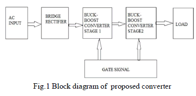
| Fig. 1 shows the block diagram of an integrated double buck–boost (IDBB) converter. The IDBB converter is proposed to supply power-LED lamps from the ac mains, providing high power factor (PF), low LED current ripple, a nd high efficiency. This converter behaves as two buck boost in cascade. The input buck boost converter is made up by Li, Di, CB, and M1, and the output buck–boost converter comprises Lo, D2, D3, C0, and M1. The reversing polarity produced by the first converter in the capacitor CB is corrected by the second converter, provide a positive output voltage with respect to ground. This simplifies the measurement of the load current for closed-loop operations. |
 |
| By operating the input inductor Li in discontinuous conduction mode (DCM), the average current through the line will be proportional to the line voltage, therefore providing a near unity PF. In the output side of converter output inductance can be operated either in continuous conduction mode (CCM) or DCM. The operation in DCM has the advantage of providing a bus voltage across CB independent of the duty cycle and output power. However, it presents the disadvantage of requiring a higher value of the output capacitance to achieve low current ripple through the load. In order to have a reduced value for the outp ut capacitance, the output inductance is operated in CCM, because the current ripple is lower in this operation mode. In addition, the operation of the second stage in CCM with a duty cycle lower than 0.5 reduces the low-frequency ripple voltage since it is multiplied by the buck–boost converter voltage ratio. In this way, it will be possible to use a film capacitor to implement the output capacitance, thus having a higher life rating and better efficiency than using electrolytic capacitors .PWM switching is used to provide pulses to the MOSFET. |
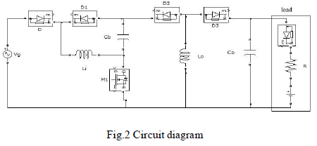 |
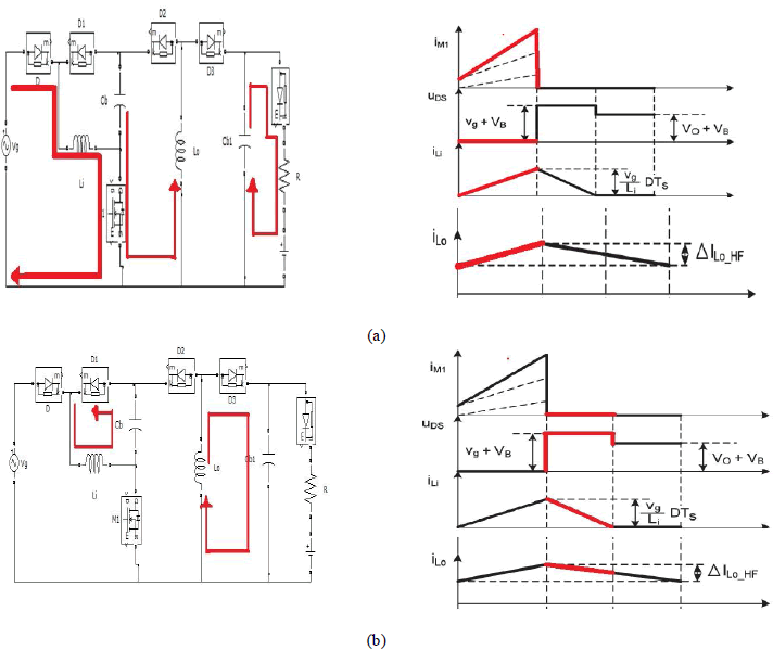
| Under the exposed operation conditions, the equivalent circuits for the operation of the IDBB converter within a switching period are shown in Fig.2. |
| Mode 1:0<t<DTs |
| The inductor Li is charged to rectified voltage Vs since the switch is on. The bus capacitor CB which is previously charged to Vs is discharged so that the output inductor is charged with bottom positive polarity. The load current is supplied by the output capacitor. |
| Mode 2:DTs<t<DTs+t1 |
| When the switch is turned off, the inductor Li is discharged through diode D1. The charge stored in the output inductor L0 is given to output capacitor Co and load through diode D3. At the end of this time inductor Li is completely discharged. |
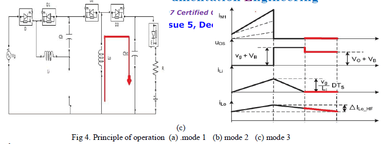
| Mode 3: DTs+t1<t<Ts |
| There is no current flow in input side. The output inductor supply the load since D3 is forward biased. |
 |
 |
| B. Analysis |
 |
 |
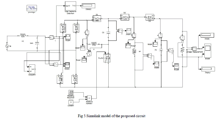
SIMULINK MODEL |
| For simulation of the proposed converter, parameters of the different circuit components are taken as: The load rating current is 350 mA, with an output power of 70W. Vγ = 170 V and Rγ = 87Ω. The equivalent load resistance at nominal power is R = 570Ω. The selected switching frequency is 50kHz. The line voltage is 230 Vrms with a 50-Hz line frequency. The converter must admit at least 10% line voltage variation, assuring constant current through the load. selecting a 45% duty cycle for the nominal operating point, a value Li = 1.7 mH is calculated. The bus capacitance CB =80uF,output inductance L0= 7mH, output capacitance Co= 40uF. |
| A. PWM Switched Model |
 |
| B. Simulation Results |
 |
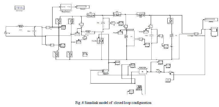
| C. Closed Loop Configuration |
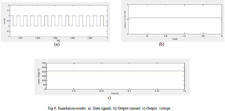
| In order to increase the performance of the system closed path is provided. PI controller is used for controller pur pose. The figure 6 shows the closed loop configuration of inverter using PI controller, with Kp=0.35 and Ki=40. Pulse is created with the help of relational operator. Direct output of relational operator is given to M1. |
 |
| D.Simulation Results |
 |
CONCLUSION |
| An IDBB converter with LC filter has been investigated to supply power for LED lighting applications. The two buck– boost converter is cascaded by using only one controlled switch. By operating the input converter in DCM, a high input PF of can be obtained. On the other hand, the operation of the second stage in CCM assures a low-ripple current through LED load without using a very high output capacitance. In this way, the converter can be implemented using only film capacitors, avoiding the use of electrolytic capacitors and increasing the converter mean time between failures. Modelling of the double buck boost converter with feedback is done and simulated the model and different waveforms are obtained. Simulation results demonstrate that the output voltage of the desired converter can be stably maintained at 200 V. Thus the proposed converter can provide high power factor upto 0.90 and good efficiency. |
References |
|