International Journal of Advanced Research in Electrical, Electronics and Instrumentation Engineering
ISSN ONLINE(2278-8875) PRINT (2320-3765)
ISSN ONLINE(2278-8875) PRINT (2320-3765)
Amrita Mariam Varghese1, Sheela Joseph2, Elizabeth Paul3
|
| Related article at Pubmed, Scholar Google |
Visit for more related articles at International Journal of Advanced Research in Electrical, Electronics and Instrumentation Engineering
This paper presents a topology for voltage step-up without the use of a converter for local electric power generation.The proposed topology contain a voltage-fed quasi-Z-source inverter on primary side, a single-phase isolation transformer, and a voltage doubler rectifier (VDR) and a single phase inverter. This paper describes the operation principles of the proposed topologies and its modelling. The performance of the topology is studied in a MATLAB/SIMULINK R2010a environment and the results are analysed.
Keywords |
| dc/dc/ac converter, VDR, PWM control |
INTRODUCTION |
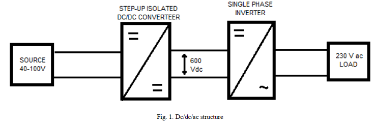
| In distributed power generation the input voltage is comparatively less than what is required ( eg. for a residential loads). So to interconnect a low-dc-voltage-producing energy sources (typically 40–80 Vdc) to residential loads (typically 230-Vac single phase or 3 × 400 Vac), a special voltage matching converter is required. A typical structure of an interface converter is shown in Fig. 1. The interface converter should be realized within the dc/dc/ac concept,due to safety and dynamic performance requirements. This means that low voltage from the source first passes through the front-end step-up dc/dc converter; then the output dc voltage is inverted in the single-phase inverter and filtered to get required output (second dc/ac stage). The design of the front-end isolated dc/dc converter is important because this stage is the main contributor of interface converter efficiencyand overall dimensions. |
 |
PROPOSED TOPOLOGY |
| A new power circuit topology is designed for the front-end dc/dc converter for distributed power generation. The topology proposed as shown in Fig. 2 contains a voltage-fed quasi-Z-source inverter (qZSI) at the converter input side, isolation transformer, a voltage doubler rectifier (VDR) and a single phase inverter |
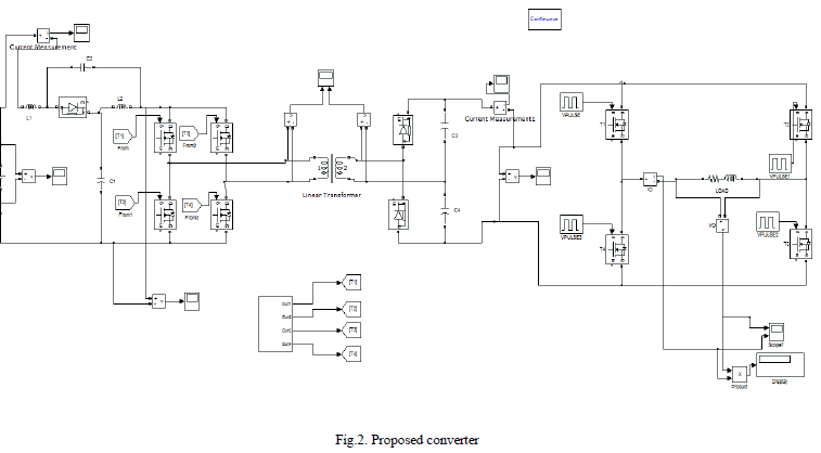 |
| The voltage-fed qZSIhas a unique feature:It can boost the input voltage by utilizing extra switching state—the shootthrough state. The shoot-though state here is thesimultaneousconductionofbothswitchesofthesamephase leg of the inverter. This operation state is forbidden for the traditional voltage source inverter (VSI) because it causes the short circuit of the dc-link capacitors. Here the shoot-through state is used to boost the magnetic energy stored in the dc-side inductors L1 and L2 without short-circuiting the dc capacitors. This increase in inductive energy, in turn, provides the boost of voltage seen on the transformer primary winding during the traditional operating states (active states) of the inverter. Thus, the varying output voltage of the source is first preregulated by adjusting the shootthroughdutycycle; then isolationtransformer (1:1)isbeing supplied with a voltage of constant amplitude value. Although the control principle of the qZSI is more complicated than that of a traditional VSI, it provides a potentially cheaper, more powerful, reliable, and efficient approach to be used for renewable energy- powered systems. |
| The voltage on the secondary of the isolation transformer is applied as input to the voltage doubler circuit (VDR) where the capacitors C3 and C4 are charged by the respective conduction of corresponding diodes hence the voltage is getting double. The output voltage is then the fed to a single phase voltage source inverter the output of the circuit can be used for residential loads and drives. |
| A. Circuit Analysis |
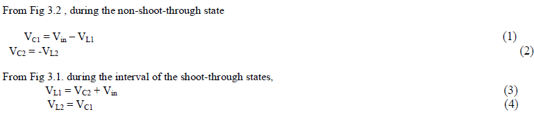
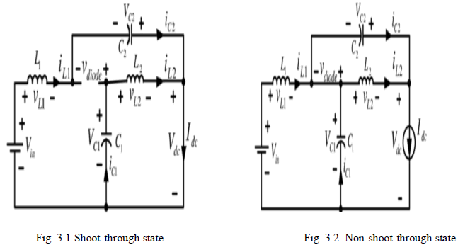
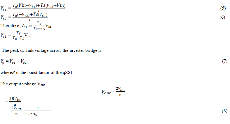
| All the voltages as well as the currents are shown in Figs 3.1 and 3.2 and the polarities are shown with arrows. Assuming that during one switching cycle, T, the interval of the shoot through state is TS; the interval of non-shootthrough states is Ta ; thus one has T = Ts + Ta1 and the shoot-through duty ratio, Ds =T0 /T. |
 |
 |
| At steady state, the average voltage of the inductors over one switching cycle is zero. |
 |
OPERATIONAL PRINCIPLE |
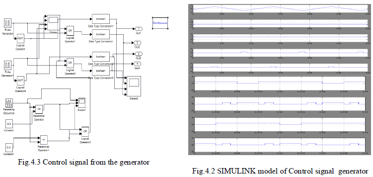
| The operating principle of the single-phase qZSI in the voltage boost operating mode is shown in the Fig. 4.1. The active states occurs in the switchingwhen only one switch in each phase leg conducts. To generate the shoot-through states, two reference signals (Up and Un) are compared with a triangular wave, if the wave is greater than Up or lower than Un, the inverter switches turn into the shoot-through state. The current through the inverter switches reaches its maximum during shoot-through. The SIMULINK model of the control structure is shown in Fig. 4.2 based on the above. The dc-link voltage and the primary winding voltage waveforms of the isolation transformer during shootthrough are shown in Fig. 4.1. The shoot-through states are created during the zero states of the full-bridge inverter, where the primary winding of the isolation transformer is shorted through either the top (T1 and T3) orbottom (T2 and T4) inverter switches. To provide a sufficient regulation margin, the zero-state time TZ should always exceed the maximum duration of the shoot-through states T0,max per one switching period |
| TZ>T,0max. (1) |
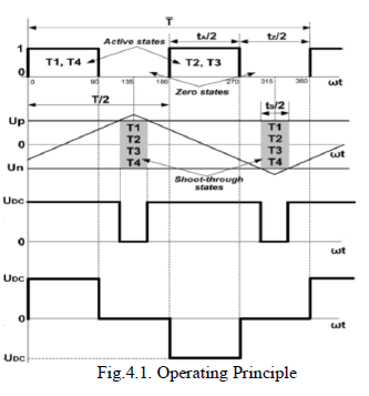 |
| Thus, each operating period of the qZSI during the shoot- through always consists of an active state T1, shoot-through state T0, and zero state TZ |
| T = T1+ T0 +TZ(2) |
| D1 + D0 + DZ = 1 (3) |
 |
SIMULATION RESULTS |
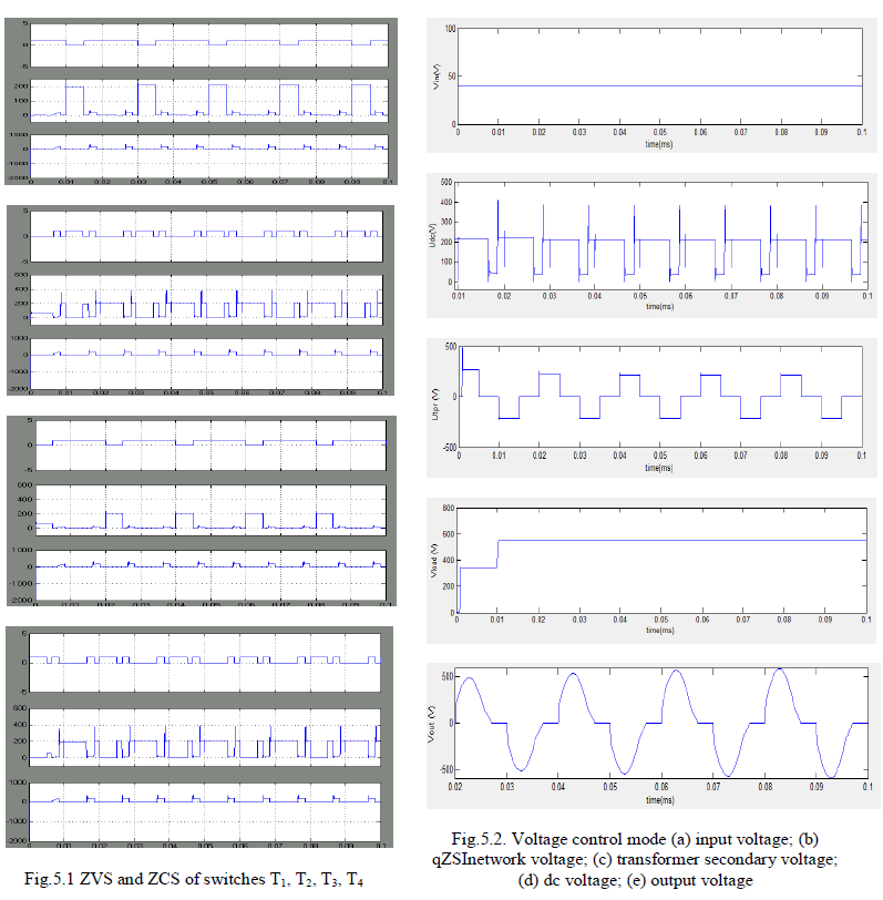
| The qZSI network causes the boost of a low dc input voltage , here an input voltage of 40V is applied which is boosted as indicated in Fig 5.2 which is applied to an isolation transformer of reduced number of turns (1:1 turns ratio). The output is then given to an inverted for the residential loads and drive applications. The switches T1and T4 shows ZCS switching while the other two switches T3 and T4 , ZVS switching which are given in the figures below |
 |
CONCLUSION |
| On primary side of transformer voltage boost function with no additional switches occurs without the use of any additional boost converters.The proposed topology boost input voltage by the shoot through operation mode and another advantage of this method isisolation transformer with reduced turns ratio is used. Can be extended to marine, aerospace applications with some modifications in circuitry. |
References |
|