International Journal of Advanced Research in Electrical, Electronics and Instrumentation Engineering
ISSN ONLINE(2278-8875) PRINT (2320-3765)
ISSN ONLINE(2278-8875) PRINT (2320-3765)
| NajibGhatte1, Vinit Pereira 2, MadurDattaprasad3, TusharSurwadkar4 PG Student [Electronics], Dept. of Electronics, Fr. Conceicao Rodrigues College of Engg.,Bandra, Mumbai, India |
| Related article at Pubmed, Scholar Google |
Visit for more related articles at International Journal of Advanced Research in Electrical, Electronics and Instrumentation Engineering
This paper talks about the indigence of Real Time Clock (RTC) for maintaining real timing constraints for various specific applications. Real time Clocking is widely and generally used in various electronic appliances so that tracking the traces becomes versatile and flexible for security purpose. Digital cameras used RTC in it so that when the image is captured it will have details of, on which day and date it was captured for future reference. Such RTCs are very useful when it comes to the need of security, cogent evidence and investigations. Microcontroller AT89C55 is programmed using I2C Protocol with Dallas RTC IC in such a way so as to maintain Real timing and same is displayed on LCD. The parameters can be varied by means of matrix keypad.
Keywords |
| RTC, I2C, LCD, keyboard, 89C55. |
INTRODUCTION |
| The whole design gives the brief idea of interfacing of Real-Time Clock to AT89C55 microcontroller using I2C protocol which works in master-slave configuration. A real time clock is basically just like a watch - it runs on a battery and keeps time even when there is a power failure. Using an RTC, it is possible to keep track of long timelines, even if microcontroller is reprogrammed or disconnected from serial bus or a power plug. Most microcontrollers, including the Arduino, have a built-in timekeeper calledmillis() and there are also timers built into the chip that can keep track of longer time periods like minutes or days. Well, the biggest reason is that millis() only keeps track of time sincethe Arduino was last powered - . That means that when the power is turned on, the millisecond timer is set back to 0. The Arduino doesn't know that it's 'Tuesday' or 'March 8th', all it can tell is 'It's been 14,000 milliseconds since It was last turned on'. |
| It becomes mandatory to program in the date and time and you it will have count from that point on. But if it lost power, it results in again resetting of the time. Much like very cheap alarm clocks: every time they lose power they blink 12:00. While this sort of basic timekeeping is OK for some projects, some projects such as data-loggers, clocks, etc will need to have consistent timekeeping that doesn't reset when the Arduino battery dies or is reprogrammed. Thus, a separate RTC is included. The RTC chip is a specialized chip that just keeps track of time. It can count leap-years and knows how many days are in a month, but it doesn't take care of Daylight Savings Time (because it changes from place to place) [1] |
DESIGN |
| The DS1307 Serial Real-Time Clock is a low-power; full binary-coded decimal (BCD) clock/calendar plus 56 bytes of NV SRAM. Address and data are transferred serially via a 2-wire, bi-directional bus. The clock/calendar provides seconds, minutes, hours, day, date, month, and year information. The end of the month date is automatically adjusted for months with fewer than 31 days, including corrections for leap year. The clock operates in either the 24-hour or 12- hour format with AM/PM indicator. The DS1307 has a built-in power sense circuit that detects power failures and automatically switches to the battery supply[2]. |
| The I2C protocol requires only 2 signals: clock and data. Clock is known as SCL or SCK (for Serial Clock), while data is known as SDA (for Serial Data). What makes I2C unique is the use of special combinations of signal conditions and changes. Fundamentally, there are just two: Start and Stop. There are some other conditions which derive from the presence or absence of these two, but they are the core of what makes this bus unique. |
| An I2C bus can potentially have multiple masters and many 'slave' devices sharing the same bus, although you rarely see multiple masters in the real world. Signal contention is avoided by means of an open-collector drive scheme, where no device will ever drive a signal high, it only drives low; for a high, the bus is pulled up by a resistor. An addressing scheme allows a device to determine if it is being queried by the master. A master sees that a slave device is present when the slave responds to its address by sending an Acknowledgement bit (driving SDA low); if no such addressed device exists, the SDA line is pulled high, and this is interpreted by the Master as a Not-Acknowledgement. |
| An IDLE bus condition is defined as having both SDA and SCL high. (This condition can exist within a bus transaction, but generally it is transitory.) A 'START" condition is generated by the Master, followed by 7 bits of address, then a ReadWrite bit. If a slave device detects an address match, it will send an ACK by driving SDA low during the next clock cycle; if no slave recognizes the address then the SDA line will be left alone to be pulled up high. Following a successful ACK, data will be either sent to the slave device or read from the slave device (depending on what was indicated by the Read/Write bit). Therefore, each byte is 9 bits: 7 address plus one R/W plus one ACK/NAK, or 8 data plus one ACK/NAK. The last data byte of a transaction should generally be followed by a NAK, to indicate that it is intended to be the final byte. After this, either a STOP or a ReSTART should be issued by the Master.[ |
IMPLEMENTATION |
| The design is simulated via Proteus ISIS v7.6 sp4 provided by Labcenter Electronics. The design is created using Schematic Capture and same is simulated. |
A. Matrix Keypad |
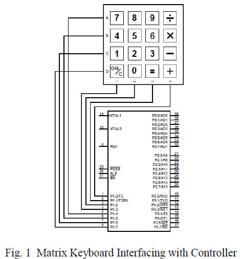
| This is a matrix of keys which responds to specific row and column. In case of matrix keypad both the ends of switches are connected to the port pin. The design has demand for a 4 × 4 matrix keyboard i. e. four rows and four columns, altogether sixteen keys, where ten keys used for numeral input and remaining six used for adjusting the real-time parameters. Thus, eight lines used to function sixteen keys. Fig. 1 shows the diagram of a matrix keypad and its interfacing with the controller. |
 |
B. Dallas DS1307 RTC |
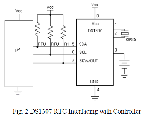
| The DS1307 is a low-power clock/calendar with 56 bytes of battery-backed SRAM. The clock/calendar provides seconds, minutes, hours, day, date, month, and year information. The date at the end of the month is automatically adjusted for months with fewer than 31 days, including corrections for leap year. The DS1307 operates as a slave device on the I2C bus. Access is obtained by implementing a START condition and providing a device identification code followed by a register address. Subsequent registers can be accessed sequentially until a STOP condition is executed. When VCC falls below 1.25 × VBAT, the device terminates an access in progress and resets the device address counter. Inputs to the device will not be recognized at this time to prevent erroneous data from being written to the device from an out-of-tolerance system. When VCC falls below VBAT, the device switches into a low-current batterybackup mode. Upon power-up, the device switches from battery to VCC when VCC is greater than VBAT +0.2V and recognizes inputs when VCC is greater than 1.25 × VBAT. Fig. 2 shows the interfacing of the DS1307 with the microcontroller. |
 |
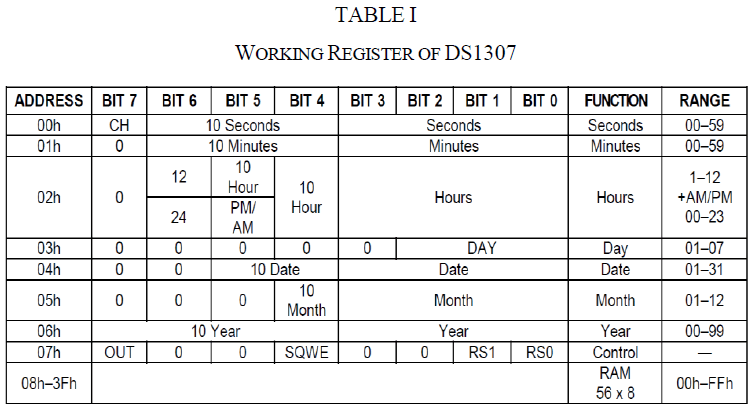
| The time and calendar information is obtained by reading the appropriate register bytes. Table I shows the RTC registers. The time and calendar are set or initialized by writing the appropriate register bytes. The contents of the time and calendar registers are in the BCD format. The day-of-week register increments at midnight. Values that correspond to the day of week are user-defined but must be sequential (i.e., if 1 equals Sunday, then 2 equals Monday, and so on.) Illogical time and date entries result in undefined operation. Bit 7 of Register 0 is the clock halt (CH) bit. When this bit is set to 1, the oscillator is disabled. When cleared to 0, the oscillator is enabled. On first application of power to the device the time and date registers are typically reset to 01/01/00 01 00:00:00 (MM/DD/YY DOW HH:MM:SS). The CH bit in the seconds register will be set to a 1. The clock can be halted whenever the timekeeping functions are not required, which minimizes current (IBATDR). |
 |
| The DS1307 can be run in either 12-hour or 24-hour mode. Bit 6 of the hours register is defined as the 12-hour or 24- hour mode-select bit. When high, the 12-hour mode is selected. In the 12-hour mode, bit 5 is the AM/PM bit with logic high being PM. In the 24-hour mode, bit 5 is the second 10-hour bit (20 to 23 hours). The hour’s value must be reentered whenever the 12/24-hour mode bit is changed. When reading or writing the time and date registers, secondary (user) buffers are used to prevent errors when the internal registers update. When reading the time and date registers, the user buffers are synchronized to the internal registers on any I2C START. The time information is read from these secondary registers while the clock continues to run. This eliminates the need to re-read the registers in case the internal registers update during a read. The divider chain is reset whenever the seconds register is written. Write transfers occur on the I2C acknowledge from the DS1307. Once the divider chain is reset, to avoid rollover issues, the remaining time and date registers must be written within one second. |
| The DS1307 supports the I2C protocol. A device that sends data onto the bus is defined as a transmitter and a device receiving data as a receiver. The device that controls the message is called a master. The devices that are controlled by the master are referred to as slaves. The bus must be controlled by a master device that generates the serial clock (SCL), controls the bus access, and generates the START and STOP conditions. The DS1307 operates as a slave on the I2C bus. |
| Data transfer can be initiated only when the bus is not busy. |
| During data transfer, the data line must remain stable whenever the clock line is HIGH. Changes in the data line while the clock line is high will be interpreted as control signals. |
| Accordingly, the following bus conditions have been defined: |
| 1) Bus not busy: Both data and clock lines remain HIGH. |
| 2) START data transfer:A change in the state of the data line, from HIGH to LOW, while the clock is HIGH, defines a START condition. |
| 3) STOP data transfer:A change in the state of the data line, from LOW to HIGH, while the clock line is HIGH, defines the STOP condition. |
| 4) Data valid: The state of the data line represents valid data when, after a START condition, the data line is stable for the duration of the HIGH period of the clock signal. The data on the line must be changed during the LOW period of the clock signal. There is one clock pulse per bit of data.Each data transfer is initiated with a START condition and terminated with a STOP condition. The number of data bytes transferred between START and STOP conditions is not limited, and is determined by the master device. The information is transferred byte-wise and each receiver acknowledges with a ninth bit. Within the I2C bus specifications a standard mode (100 kHz clock rate) and a fast mode (400 kHz clock rate) are defined. The DS1307 operates in the standard mode (100 kHz) only. |
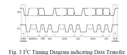
| 5) Acknowledge: Each receiving device, when addressed, is obliged to generate an acknowledge after the reception of each byte. The master device must generate an extra clock pulse which is associated with this acknowledge bit. A device that acknowledges must pull down the SDA line during the acknowledge clock pulse in such a way that the SDA line is stable LOW during the HIGH period of the acknowledge related clock pulse. Of course, setup and hold times must be taken into account. A master must signal an end of data to the slave by not generating an acknowledge bit on the last byte that has been clocked out of the slave. In this case, the slave must leave the data line HIGH to enable the master to generate the STOP condition. Fig. 3 shows the timing diagram indicating the data transfer using I2C protocol by SDA and SCL.[1] |
 |
C. Alphanumeric LCD |
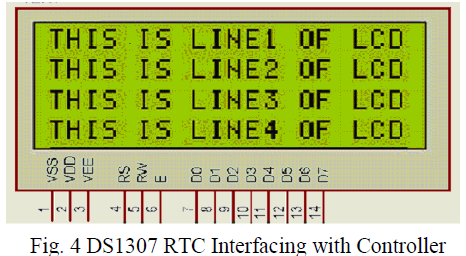
| LCD's are very simple to interface with the controller as well as are cost effective. The ALPHANUMERICdisplay used in proposed design here is 4× 20(four lines & twenty characters per line) as shown in Fig. 4.The LCD requires 3 control lines (RS, R/W & EN) & 8 (or 4) data lines. The number on data lines depends on the mode of operation. If operated in 8-bit mode then 8 data lines + 3 control lines i.e. total 11 lines are required. And if operated in 4-bit mode then 4 data lines + 3 control lines i.e. 7 lines are required. How do we decide which mode to use? It’s simple if you have sufficient data lines you can go for 8 bit mode & if there is a time constrain i.e. display should be faster then we have to use 8-bit mode because basically 4-bit mode takes twice as more time as compared to 8-bit mode. |
 |
| When RS is low (0), the data is to be treated as a command. When RS is high (1), the data being sent is considered as text data which should be displayed on the screen. When R/W is low (0), the information on the data bus is being written to the LCD. When RW is high (1), the program is effectively reading from the LCD. Most of the times there is no need to read from the LCD so this line can directly be connected to GND thus saving one controller line. The ENABLE pin is used to latch the data present on the data pins. A HIGH - LOW signal is required to latch the data. The LCD interprets and executes command at the instant the EN line is brought low. If EN is not instantiated, instruction will never be executed. [5] |
D. Microcontroller AT89C55 |
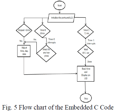
| The AT89C55WD is a low-power; high-performance CMOS 8-bit microcontroller with 20K bytes of Flash programmable read only memory and 256 bytes of RAM. The device is manufactured using Atmel’s high-density nonvolatile memory technology and is compatible with the industry standard 80C51 and 80C52 instruction set and pinout. The on-chip Flash allows the program memory to be user programmed by a conventional non-volatile memory programmer. By combining a versatile 8-bit CPU with Flash on a monolithic chip, the Atmel AT89C55WD is a powerful microcomputer which provides a highly flexible and cost effective solution to many embedded control applications.The microcontroller is programmed with Embedded C language using Keil cross-compiler and Intel-hex file is generated and embed into the controller to simulate the results.Fig. 5 shows the embedded code flow-chart. Microcontroller is embedded with the generated hex file and design is simulated to get optimum results. |
 |
RESULTS |
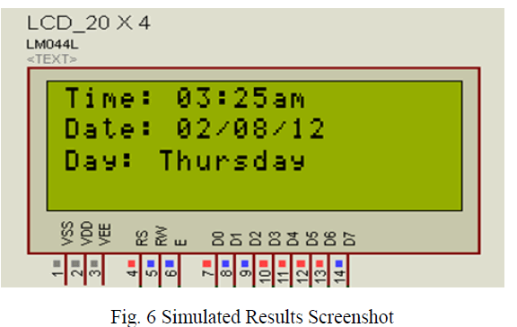
| The proposed design is simulated on the simulation platform. The alphanumeric LCD displays the time, date, day as outsourced by the RTC. The parameters can be changed by means of matrix keypad thus interfaced and optimum results were obtained. Fig. 6 shows the display of the LCD as per anticipation. |
 |
CONCLUSIONS |
| Real time programming using I2C protocol with RTC was successfully implemented which helps to maintain real time clock necessary for various real time running systems like mobile phones, hospitals etc. It even satisfies the need in military applications with providing some features of changing the timing and date as per necessity. |
References |
|