Research & Reviews: Journal of Material Sciences
ISSN:2321-6212
ISSN:2321-6212
1Department of Physics, Alabama A&M University, Normal, Al 35762, USA
2Department of Physics and Dual Degree Engineering, Xavier University of Louisiana, USA
Received date: 03/02/2017; Accepted date: 20/02/2017; Published date: 28/02/2017
Visit for more related articles at Research & Reviews: Journal of Material Sciences
There are numerous applications for the pyroelectric composite films in the medical field, military field and environmental applications field. The main focus of this research is to fabricate the higher efficiency thin films that are flexible like the polymers. PVDF is ideal when it comes to making detectors as they are flexible; possess high pyroelectric current and resistance, low dielectric constant and density. Pure PVDF and PVDF films doped with CNT and MWCNT, PVDF: LiTaO3, PVDF: LiTaO3 films doped with MWCNT thin films were fabricated using the solution casting technique. Films fabricated were characterized for their electrical, optical and structural properties using FTIR Spectroscopy, UV-Vis Spectroscopy, and Raman Spectrum. From UV-Vis spectroscopy analysis it is calculated that the indirect bandgap energy of pure PVDF is 5.99 eV, 4.85 eV for PVDF+0.5%-CNT, 4.76 eV for PVDF+1%-CNT, 5.22 eV for PVDF+LT, 4.95 eV for PVDF+LT+2%-MWCNT and 4.85 eV PVDF+LT+2.5%-MWCNT. The calculated direct bandgap energy of pure PVDF is 6.25 eV, 5.95 eV for PVDF+0.5%-CNT, 4.85 eV for PVDF+1%- CNT, 5.42 eV for PVDF+LT, 5.12 eV for PVDF+LT+2%-MWCNT and 4.95 eV PVDF+LT+2.5%-MWCNT. The decrease in the bandgap may be attributed to the presence of unstructured bulk defects. Obtained results show that doping of PVDF and its nanocomposite materials with CNT and MWCNT is enhancing the key characteristics of the materials that are beneficial for the optical devices industry.
Pyroelectric infrared sensor; Polycrystalline ceramics; Multi-layer ceramic capacitors; Irradiation; Structural modification
Polyvinylidenefluoride (PVDF) is a polymer with great flexibility, mechanical robustness, and chemical resistance, along with attractive dielectric and pyroelectric properties. PVDF attracted because of its distinguished electroactive properties, nonlinear optical, strong corrosive, susceptibility, and high dielectric constant [1,2], which make it useful in a variety of fields such as sensors, actuators, and energy transducers [3]. Some devices made up of PVDF also require high voltage power source that may be a limiting factor for several applications. Hence, composition polymer matrix and ceramic fiber is likely to alleviate assets regarding both mechanical and piezoelectric responses. Composite film consists of at least two compounds is preferred over one compound alone if it exhibits more favorable figures of merit [4,5]. Recent studies show that the composite films are better for use in infrared detectors and other technology relying on smart materials than pure films. Reports indicate that the materials processed by PVDF/PZT composite films and demonstrate an increase in the peak polarization compared to plain PVDF [6]. The fabrication of composites is the preliminary phase where the feasibility of the approach is evaluated by the electromechanical characterization on the composite films. The polymer matrix material PVDF is used in polymer solution. Reports indicate many techniques for fabricating thick films of PVDF and PVDF: Nanocomposite materials. Recent studies show sol-gel technique [7], electrospinning [8], dip coating, [9], and screen printing [10], laser ablation [11], and spin coating [12] for fabrication of thin and thick films [13]. Solution casting technique is used in the current work due to its ease of fabrication and cost effectiveness [14]. Solution casting method is been used by many scientists and Manjunatha et.al, and Santhosh K. Y. et.al reported the efficiency of the films fabricated by this particular method [15,16].
Most of the PVDF's piezoelectric characters are due to the β phase that has the largest spontaneous polarization per unit cell and thus, exhibits the highest electroactive properties [15]. It is reported that electrospinning and blending PVDF with carbon nanotubes (CNTs) can increase the β-phase content in PVDF [16]. Combining organic polymers with PVDF enhances the optical properties of nanocomposites. Although numerous studies on PVDF/CNT nanofibrous composites have been reported, new fascinating results have been emerging consistently and continually [17]. In the present work, well-aligned PVDF with different CNTs weight percentages and nanocomposite materials with lithium tantalate (LiTaO3) and PVDF+LiTaO3 doped with various multi-walled carbon nanotube (MWCNT-multiple layers of graphite, rolled in onto them to form a tube shape structure) weight percentages have been fabricated using a solution casting method. Obtained films were characterized for their optical characteristics to find their usefulness in the field of optoelectronic devices. The study of dielectric and optical properties of these composite materials is important as the properties of those materials vary from the individual constituents and varies with the fraction of the filler. Sometimes these properties are greater than the filler and the matrix.
Optical Characteristics
In recent years, polymers with different optical properties have been attracted much attention due to their applications in the sensors, optical devices, and LEDs, etc. The optical properties of these materials can be easily tuned by controlling the dopant materials and optimizing the dopant concentrations. The optical characterization is very important as the absorbance, transmittance and reflectance of the polymeric films are the key optical parameters which are used in deducing the other important characteristics such as extinction coefficient, energy gaps, optical loss, and dielectric constants etc. In the present work, the absorption coefficient, refractive index, extinction coefficient and real and imaginary parts of dielectric constant were determined, and the effect of CNT and MWCNT on some of its optical properties is studied along with Raman, FTIR studies.
The study of the absorption process is nothing but the analysis of light and electrons interaction [18,19]. Photon is absorbed when its frequency matches with the excited electron that would was allowed to higher state [20], otherwise the material is transparent to such radiation. Semiconductors’ optical properties lie between metals and insulators (dielectrics). In order to make the dielectrics perform as good as conductors for the specific purposes the doping process is used and presence of dopants may change the optical properties of these materials [21]. Due to the very reason the PVDF, LiTaO3 dielectrics, semiconductor crystalline materials are considered for research. Current research emphasizes on the addition of CNTs and Multi-wall Carbon Nanotubes (MWCNTs) to PVDF and also PVDF pairing up with other bulk pyroelectric materials to form a thick film. CNT consist of graphite rolled in the form a tube shape structure. MWCNT consist of multiple layers of graphite, rolled in onto them to form a tube shape structure. MWCNTs of outside diameter × length (7-15 nm × 0.5-10 μm, respectively) exhibit excellent mechanical and electrical properties. Absorption coefficient (α), is the measure of the rate of decrease in the intensity of electromagnetic radiation as it passes through a given substance [22].
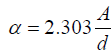 (1)
(1)
where, d= film thickness in cm and A= log (I0/I) where I0 and I are the intensities of the incident and transmitted beams respectively.
The absorption edge for direct and non-direct transitions can be obtained in view of the models proposed by Tauc’s relation [23],
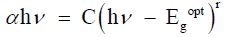 (2)
(2)
where, α=absorption coefficient, ν=frequency, h=Planck’s constant, C=speed of light through air/vacuum,  is the optical
energy bandgap between the valence band and the conduction band and r is the power that characterizes the transition process.
is the optical
energy bandgap between the valence band and the conduction band and r is the power that characterizes the transition process.
The reflectance (R- measures of what proportion of light, is reflected off of the substance) has been found from values of transmission (T), and Absorbance (A), using the relationship:
A+R+T=1 (3)
For normal reflectance, the refractive index can be determined from the relation:
 (4)
(4)
The extinction coefficient k is related to the absorption coefficient α by the relation:
 (5)
(5)
where, λ is the incident photon wavelength.
The relation between the complex dielectric constant and the complex refractive index N is:
Expressed by:
ε = N2 (6)
It can be concluded that:
(n-ik)2 = ε′ - ε″ (7)
The real (εr) and imaginary (εi) parts of the dielectric constant thus related to (n) and (k) values and can be calculated using the following formulas [19]:
ε′ = n2 -k2 and ε″ = 2nk (8)
The above equations relate to the energy stored and the energy dissipated by the medium respectively.
Optical loss 
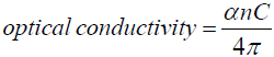
Optical conductivity can be calculated by finding the ratio of nC and 4π, and this property is used to describe a materials response to electromagnetic waves.
Optical density, which represents the degree to which transmitted light retards in a material, is determined by the equation:
Optical density = αd (11)
Materials Used and Films Preparation
PVDF, MEK, DMF, LiTaO3, CNT, and MWCNT were purchased from Sigma-Aldrich. A typical Flowchart of 0-3 connectivity thinand thick- films of nanocomposite prepared using the solution casting method is described in Figure 1.

Figure 1: A Flow Chart for Fabrication of Films.
Fourier Transform Infrared (FTIR) Spectroscopy Studies
Infrared vibrational spectroscopic study was carried out to characterize the optical characteristics of PVDF, PVDF: LiTaO3, PVDF doped with CNT and PVDF+LiTaO3 doped with MWCNT films. FTIR is a technique which is used to obtain an infrared spectrum of absorption or emission of a solid, liquid or gas. An FTIR spectrometer simultaneously collects high spectral resolution data over a wide spectral range. This confers a significant advantage over a dispersive spectrometer which measures intensity over a narrow range of wavelengths at a time. The term Fourier transform infrared spectroscopy originates from the fact that a Fourier transform (a mathematical process) is required to convert the raw data into the actual spectrum.
In order to understand the existence of dopants and its bonding nature, the FTIR spectrum is analyzed. Figure 2 shows the comparison of wave number vs. transmittance of PVDF samples with various doping, according to the data obtained; The peak at 450 cm−1 is the characteristic peak of the β-phase of PVDF, peak at 525 cm−1 band is assigned to a CF2 bending mode, and the peak at 745 cm−1 is assigned to a rocking mode [24-26]. PVDF has peaks at 879 cm-1 which is assigned to a mixed mode of CH2 rocking and CF2 asymmetric stretching vibration [24-26], 1289 cm-1 is assigned to CH2 Out-of-plane bending which is also referred as wagging or twisting and 1479 cm-1. Similarly, PVDF+CNT-1%, PVDF+CNT-0.51%, PVDF+MWCNT-2% has less intense peaks at the same locations that confirms the existence of C-C bonds present in the samples. The characteristics peaks obtained at 445 cm-1, 525 cm-1, 745 cm-1 and 879 cm-1 corresponding to the β-phase of PVDF which is the crystalline region of the PVDF. This phase dies down towards the high wave number region implying the decrement in the crystalline phase of the polymer matrix after 2000 cm-1. There is a slight increase in the peals around 2800 cm-1 that corresponds to the amorphous phase of the host polymer. Peaks at 2960 cm-1 and 2990 cm-1 are related to the asymmetric and symmetric stretching vibration of methyl groups. Symmetric vibrations are generally weaker than asymmetric vibrations since the former lead to less of a change in dipole moment [27].

Figure 2: Comparison of Wave Number vs. Transmittance of PVDF samples with various doping.
Figure 3 shows the comparison of wave number vs. transmittance of PVDF samples with LiTaO3 and MWCNT doping, according to the data obtained, PVDF has peaks at 679 cm-1, 1179 cm-1, 1439 cm-1, 1689 cm-1, and 2029 cm-1 which are the characteristic peaks of PVDF corresponding to the α and β-phases of PVDF [28-30]. Similarly, PVDF+LiTaO3, PVDF+LiTaO3+MWCNT have higher intense peaks at the same locations that confirm the existence of CH2, CF2, C-C bonds and C-O bonds in the samples. As the PVDF has various peaks based on the various symmetric and asymmetric stretching, the graph shown Figure 3 has peaks.

Figure 3: Comparison of Energy vs. Transmittance of PVDF: Nanocomposites.
Figure 4 shows the comparison of wave number vs. Log(1/R) of PVDF samples with various doping, according to the data obtained, PVDF has peaks at 639 cm-1, 729 cm-1, 849 cm-1, 1041 cm-1, 1241 cm-1, and 1479 cm-1. Similarly, PVDF+CNT-0.5%, PVDF+CNT-1%, PVDF+MWCNT-2%, and PVDF+ MWCNT-2.5% has much lesser intense peaks at the same locations that confirm the existence of C-C bonds and C-O bonds in the samples. These peaks match with the characteristic peaks of CNT and MWCNT. The intensity of the peaks in Figure 4, decrease with the increased amount of the dopant in the polymer matrix.

Figure 4: Comparison of Wave number vs. Log (1/R) of PVDF samples with various doping.
Figure 5 shows the comparison of wave number vs. Log (1/R) of PVDF samples with LiTaO3 and MWCNT. various doping, according to the data obtained, PVDF has peaks at 579 cm-1, 669 cm-1, 849 cm-1, 1041 cm-1, 1121 cm-1, 1241 cm-1, 1479 cm- 1, 1689 cm-1, and 2629 cm-1, and 2979 cm-1. Similarly, PVDF+LiTaO3, and PVDF+LiTaO3+MWCNT have much higher intense peaks at the same locations that confirm the existence of C-C bonds and C-O bonds in the samples. These peaks match with the characteristic peaks of CNT and MWCNT. The intensity of the peaks in Figure 6, increase with the increased amount of the dopant in the polymer matrix [31-33].

Figure 5: Comparison of Wave number vs. Log (1/R) of PVDF: Nanocomposites.

Figure 6: Comparison of Wave Length vs. Absorption Coefficient (α) of the Samples with Various Doping.
UV-VIS Transmission Spectral Analysis
The optical property of the material gives information regarding the composition nature of the material. Because molecules absorb different wavelengths of light depending on their structures, the molecular structure of a compound can be identified by monitoring the percentage of absorbance or reflectance. Data obtained from the spectrometer can not only help identify the bonds between the molecules of the crystal, but can also help us calculate the optical properties that include bandgap energy, optical loss, optical density, dielectric constants, dielectric loss, etc [34-37]. The results presented in this research give the details of the electronic structure of the optical bandgap. All the graphs presented here on exhibit all around superior properties when doped by CNT or MWCNT.
The absorption spectra of the pure PVDF, PVDF+CNT, PVDF+LiTaO3, and PVDF+LiTaO3+MWCNT are shown in Figures 6 and 7. From Figures 6 and 7 it is evident that the PVDF and doped PVDF along with PVDF: nanocomposites display an excellent transmission in the entire UV–vis region. Figure 8 also portrays the enhanced percentage transmittance as the increase in the dopant percentage compared to the pure PVDF. Enhanced percentage absorption is a very important property for optoelectronic applications.

Figure 7: Comparison of Energy vs. Absorption Coefficient (α) of the Samples with Various Doping.

Figure 8: Comparison of Energy (hν) vs. (αhν)1/2 Of the Samples with Various Doping.
The study of the absorption spectrum is very important as it gives the details of the band structure and whether it is affected near the band extreme or not. So using Tauc’s relation, plot in Figure 8 is used to find the indirect bandgap by extrapolating the linear portion of the curve to zero. The indirect bandgap energy was found to be 5.99 eV for pure PVDF, 4.85 eV for PVDF+CNT-0.5%, 4.76 eV for PVDF+CNT-1%, 5.22 eV for PVDF+LT, 4.95 eV for PVDF+LT+MWCNT-2% and 4.85 eV PVDF+LT+MWCNT-2.5%. The decrease in the optical indirect bandgap values is due to the formation of the defects, and consequently influences the optical properties of the materials [38-40].
Figure 9 show the graph energy versus (αhν)2 through it is very clear that as the photon energy is increasing the (αhν)2 is
increasing. From the plots of energy vs. (αhν)2 we can find out the direct bandgap energy of the samples by extrapolating the
linear portion of the curve to zero. The determination of the value of optical energy bandgap  involves the plotting of (αhν)1/2 against hν. The direct and indirect optical bandgap energies can be determined by plotting photon’s energy and extrapolating the
linear portion of the curve towards zero. The optical bandgap energy Ea is the energy difference between the top of the valence
band and bottom of the conduction band of electrons. The optical activation energy, which is the energy required for a particle to
overcome a potential barrier, was extrapolated from the linear portion of the curve of the natural log of the absorption coefficient
vs. the energy to zero.
involves the plotting of (αhν)1/2 against hν. The direct and indirect optical bandgap energies can be determined by plotting photon’s energy and extrapolating the
linear portion of the curve towards zero. The optical bandgap energy Ea is the energy difference between the top of the valence
band and bottom of the conduction band of electrons. The optical activation energy, which is the energy required for a particle to
overcome a potential barrier, was extrapolated from the linear portion of the curve of the natural log of the absorption coefficient
vs. the energy to zero.

Figure 9: Comparison of Energy vs. (αhν)2 Of the Samples with Various Doping.
Using Tauc’s relation, plot in Figure 9 is used to find the direct bandgap by extrapolating the linear portion of the curve to zero. The intercepts (extrapolations) of the best fit line on energy axis will give the value of direct optical energy bandgap. The direct bandgap energy was found to be 6.25 eV for pure PVDF, 5.95 eV for PVDF+CNT-0.5%, 4.85 eV for PVDF+CNT-1%, 5.42 eV for PVDF+LT, 5.12 eV for PVDF+LT+MWCNT-2% and 4.95 eV PVDF+LT+MWCNT-2.5%. From the results it is clear that the due to the increased irregularity that is caused by doping, there is a small decrease in the optical bandgap values. Thus behavior may be associated with the structural changes occurring after adding the composite material or the dopants. Hence it is concluded that the optical bandgap is compositional dependant and especially dopant dependent. From the direct bandgap energy values and indirect bandgap energy values it its evident that the direct bandgap values are higher than the indirect bandgap values [41].
The extinction coefficient, determines how fast the amplitude of the wave decreases. From Figure 10 it is evident that as the wave length is increasing the extinction coefficient is also increasing. Due to the doping, the density of the samples increases which might be the primary reason for the increase in the extinction coefficient. As depicted in Figure 11 the real part of dielectric constants increase as the photon’s energy increases. The increase in the dielectric constant is with an increase in the volume fraction of the CNT/MWCNT is attributed to an increase in dipolar polarization especially in the high frequency regime. This extra polarization possibly arises from the space charge polarization. The real part indicates how the speed of light in the material can be slowed down while the imaginary part deals with the absorption of energy by a dielectric from electric field due to dipole motion. The imaginary part deals with the absorption of energy by a dielectric from electric field due to dipole motion. The increase in the dielectric loss tangent in low energy levels region may be described by the formation of conducting path through capacitance network [42].

Figure 10: Comparison of Extinction Coefficient of the Samples with Various Doping.

Figure 11: Comparison of Real Part of Dielectric Constant of Samples with Various Doping.
It is observed that there is an increase in the imaginary part of the dielectric constant is very small compared to the increase in the real part of the dielectric constant. The results show that the samples follow the standard ferroelectric materials characteristics. Doping with CNT is not leading to increase in the dielectric characteristics but doping with MWCNT is leading to increase in the dielectric constants in a drastic way.
Compared to pure PVDF, PVDF+LT have about 3 times higher dielectric constant values which will make the material useful when high dielectric constant material are needed for specific applications. Imaginary part of the dielectric constant of PVDF+LT is about 4 times higher than pure PVDF. The optical loss is a greatly desired quality in materials and it is evident from the graph shown in Figure 12 that as the energy is increasing the optical loss is decreasing and doping with CNT and LiTaO3 is not changing the material property that is decrease in the optical loss as the energy increases but in the value of optical loss increases very minimally as the doping quantity is increased (Figure 13). The optical conductivity is one of the powerful tools for studying the electronic states in materials. The plot between the optical conductivity against photon energy is depicted in Figure 14. The spectrum indicates that optical conductivity increases with the increase of photon energy. Due to the decrease in the direct bandgap by the addition of the dopants the optical conductivity increases. It is very clear from the graph that the optical conductivity is increasing with the increase in the doping of material and its quantities [43]. The behavior of optical density is similar to the variation of optical conductivity with photon energy in pure and doped PVDF as shown in Figure 15.

Figure 12: Comparison of Optical Loss of the Samples with Various Doping.

Figure 13: Comparison of ln α of the Samples with Various Doping.

Figure 14: Comparison of Optical Conductivity of the Samples with Various Doping.

Figure 15: Comparison of Optical Density of the Samples with Various Doping.
Thin films of PVDF, PVDF+CNT-0.5%, PVDF+CNT-1%, PVDF+LT, PVDF+LT+MWCNT-2%, and PVDF+LT+MWCNT-2.5% were fabricated using the solution casting method successfully at Department of Physics, AAMU. All these films were characterized for their electrical and optical properties. From the results it is evident that doping PVDF with CNT or MWCNT is enhancing the electrical and optical characteristics of the pure material. FTIR results show the details of the functional groups present in the material and also were matched with the literature. The optical characteristics such as the optical bandgap (direct and indirect), absorption coefficient (α), extinction coefficient (k), and real and imaginary dielectric constants (ε' and ε''), optical density, optical loss (tan δ), optical conductance, and ln (α) were calculated to analyze the optical properties of pure and doped PVDF and PVDF+LT nanocomposite thin films. The doped PVDF and doped PVDF+LT nanocomposite thin films have higher transparency than those pure PVDF thin films in the UV-Visible region with good optical constants making them useful for photonic device applications.
Based on the current results it is clear that doping PVDF and PVDF nanocomposites with CNT/MWCNT has a great impact on the electrical and optical characteristics. In future the research will be concentrated on the optimal amount that need to be added to obtain best set of results that are needed by the optical device and other applications.
This work has been supported by DHS-BS Award #2010-ST-062-000034 and NSF Awards #1546965, and #1546965. Authors also thank Dr. A. K. Batra for his help in every aspect of this research.