Keywords
|
| Conservative logic, Reversible gate |
INTRODUCTION
|
| Conservative logic is a logic which reflects the property that there is equal number of one’s in the inputs as well as in the outputs[1]. It can be reversible or irreversible in nature. Reversibility is nothing but the circuit exhibits one-to-one mapping between input and output vector, and also represents for each input vector there is an unique output vector and vice versa. Conservative logic is said to be reversible only when the circuit possess the above property of reversibility .Otherwise, conservative logic is irreversible. Reversibility is mainly preferred because it can provide the methodology for designing low power circuits. Any sequential circuit can be tested by having only two test vectors (all 1’s and all 0’s) when the circuit is based on conservative logic. The designs of latches, flip flops are presented based on reversible conservative logic gate. |
| There are number of existing reversible logic gates such as Fredkin gate, Feynman gate, Peres gate, Tofolli gate. Fredkin gate is used for designing such testable sequential circuit is presented, thereby avoiding the usage of scan path access to the internal memory cell [2]. Henceforth, testing time can be reduced. Testable sequential circuit can have normal mode and test mode. In the normal mode, the circuit will have feedback but in the test mode, the circuit is made as suitable by disrupting the feedback. So, the circuit is to be tested by only two test vectors (0’s and 1’s). |
| This paper involves: Section II represent the fundamentals such as Reversible Fredkin gate, and the Conservative logic. Section III represents testable sequential circuits such as reversible gate based latch and reversible gate based flip flops. Section IV shows the simulation results and Section V represents the conclusion. |
FUNDAMENTALS
|
Reversible fredkin gate
|
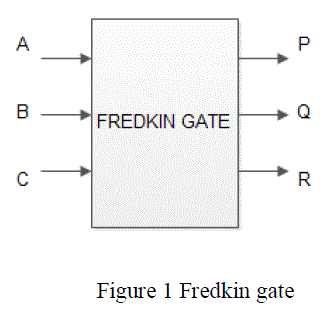
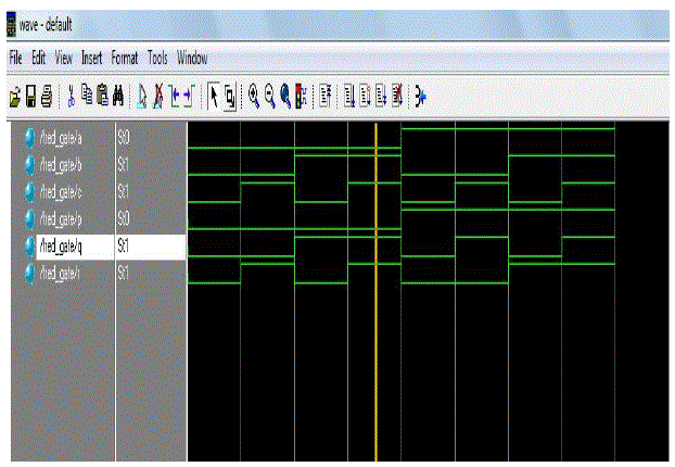
| Reversible gate is a logical gate with one-to-one mapping i.e., for each input vector, there is a unique output vector and vice versa. Also known as reversible conservative logic. Fanout at the output is not allowed. The designs presented in this paper are based on conservative reversible (three inputs: three outputs) Fredkin gate shown it can be described as mapping (A,B, and C) to (P = A,Q = AB + AC, and R = AB + AC),where A,B, and C are the inputs, and P,Q, and R are the outputs, respectively. The operation involves: Whenever the first input (say A) is 1, the swapping of inputs B and C is done at the output. Otherwise, output is same as input. Table I shows the truth table of Fredkin Gate, and it can be seen that Fredkin gate produces the same number of 1’s in the outputs as on the inputs, in addition to the one-to-one mapping feature of reversibility. |
Conservative logic
|
| A conservative-logic gate is any Boolean function that is invertible and conservative. It is well known that, under the ordinary rules of function composition (where fan-out is allowed), the two-input NAND gate constitutes a universal primitive for the set of all Boolean functions. In conservative logic, an analogous role is played by a single signalprocessing primitive, namely, the Fredkin gate, defined by the truth table. |
| This computing element can be visualized as a device that performs conditional crossover of two data signals according to the value of a control signal. When the control signals, say A is 1, swapping of B and C is done and is reflected at the output. Otherwise, Output is same as that of input only when A is 0.Observe that the Fredkin gate is nonlinear and coincides with its own inverse. Any output of a gate can be connected only to the input of a wire, and similarly any input of a gate only to the output of a wire. |
TESTABLE SEQUENTIAL CIRCUITS: LATCHES AND FLIP FLOPS
|
| The sequential circuits are made suitable to be tested by only two test vectors. Fredkin gate is used to design those sequential circuits[5]. Therefore the circuit is suitable for testing thereby scan path access is not required and testing time is reduced finally. Sequential circuits say Latches and flip flop (DET flip flop and Master-Slave flip flop) are considered. |
Reversible gate based D Latch
|
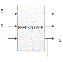
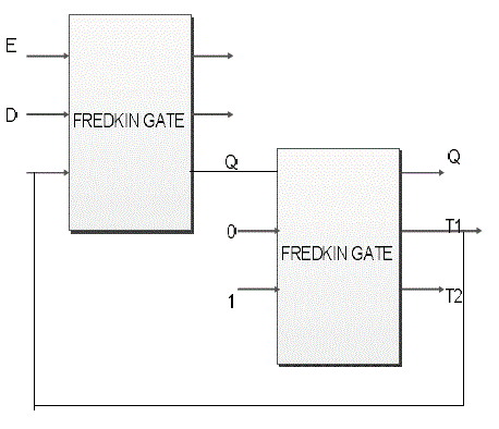
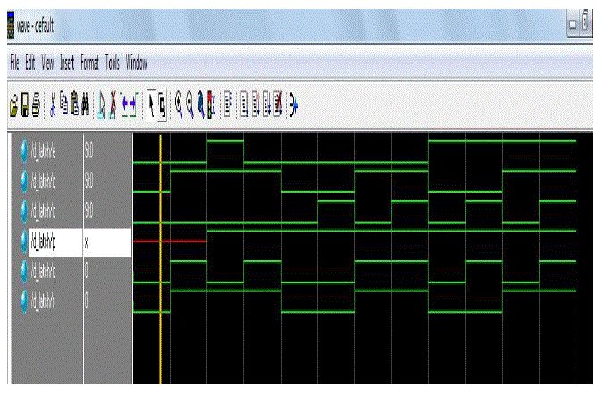
| Latch is the basic element used to store the data in digital design. Sequential circuits are mainly preferred mainly preferred because of its memory. D latch is considered in this paper, designed by using reversible gate say the fredkin gate and tested by all zero’s and all one’s shown in the figure 2. This is coded by the VHDL language and then simulated. This circuit involves normal mode and test mode. |
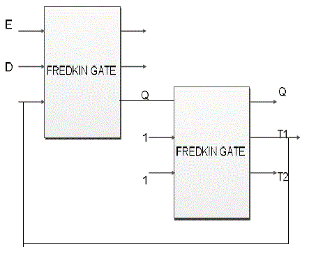
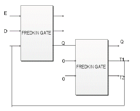
| In the Normal mode, control signals (say C1 and C2) are set to 01.Then the sequential circuit will operate as D latch without any fan-out problem. Test mode involves control signals which are set to C1C2=00(all 0’s).So that the design can be tested with the respective vector. Thus stuck at 1 fault can be detected. It is same as that for the stuck at 0 faults to be detected; both the C1 and C2 are set to 11. Then the design will disrupt the feedback in test mode and take care of the fanout. |
| The Reversible gate based circuit with the respective control signals are shown in the figure 3,4,5. Unidirectional stuck at fault are then detected. These two test vectors are long enough to detect all faults present in the circuit. |
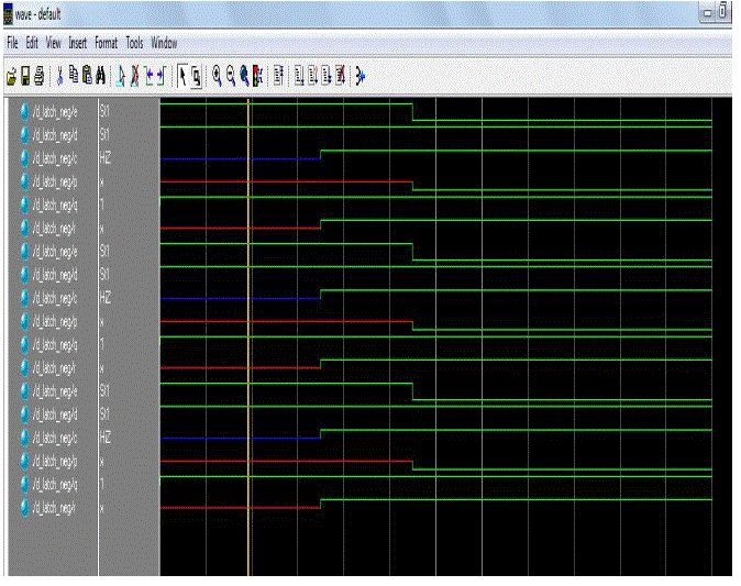
| The negative enable D latch is also coded and tested by using the test vectors. It is illustrated in the figure 6.This latch is activated only when the enable is negative or E=0.In this design, the second fredkin gate will take care out of the fan out and the design can be tested. |
Reversible gate based Master slave D flip flop
|
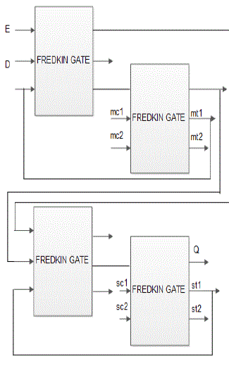
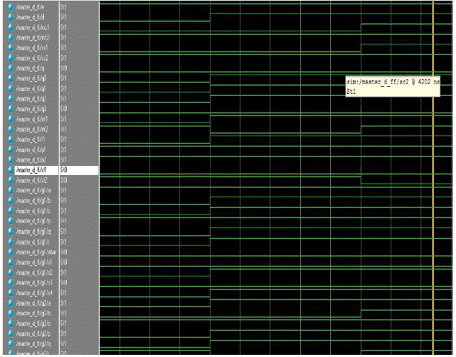
| Flipflop is another storage element used to store one bit of information. The only difference between latch and flip flop is that enable signal. Flip flops such as Master-slave flip flop and DET flipflop are considered to design the testable sequential circuits Fredkin gate is used in order to make the design to be tested by two test vectors. Like the Reversible gate based D latch, this design consists of normal mode and test mode. Hence the faults are detected and the testing time is reduced rather than the designs are tested using the scan path. For the Master slave D flip flop, the figure 7 represents consist of Positive enable D latch acts as master and slave where the negative enable D latch is acts as slave. The control signals mc1, mc2, sc1 and sc2 are set to 01. The control signals are set to 01 for the normal mode. |
| In the test mode, all the stuck at 0 fault can be detected by setting the control signals(mc1,mc2,sc1,sc2) to 1111.Likewise, all the stuck at 1 fault can be detected by passing the test vector of all zeros (i.e.)0000.D flipflop is considered for this design because the output is preserved from its input. The wholesome design can be implemented using the fredkin gate since it is a reversible gate. The reason is that reversible gate exhibits low power dissipation compared to the CMOS. Both the test vectors 0000 and 1111 will break the feedback in the test mode. |
Reversible gate based DET flipflop
|
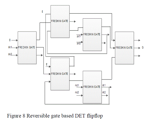
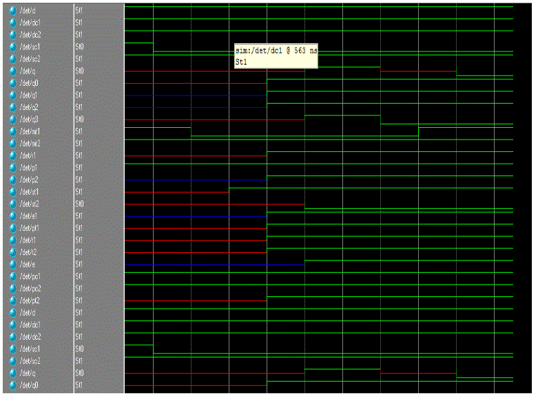
| The above design method is same as that for designing the DET flipflop which is coded and simulated by modelsim. In the Master slave flipflop, the sampling and storing the input data at both positive and negative edges (the rising and the falling edge) of the clock cannot be possible. In order to overcome this, DET flipflop is used (illustrated below). The advantage of this design is that the data rate can be maintained and frequency is reduced to half when compared with the master slave flipflop.This design is illustrated above(figure 8). The design consists of positive enable and negative enable flipflop along with the 2:1 mux at the output to pick one of the results from the design. Both the positive enable flipflop, negative enable flipflop are in parallel but the fan out is not allowed since it is reversible and control signals such as pc1,pc2,nc1,nc2. The same procedure is applied for the test mode and normal mode. |
CONCLUSION
|
| Sequential circuits are basically used for testing. Instead of scan path access to the internal memory cell, the circuits are designed by the reversible gate especially fredkin gate. The designs of reversible gate based latch, flipflop are made. Since those circuits are based on conservative logic and the circuits are made to be changed by reversible gates, the entire design can detect all possible stuck at 1 fault that can be found by having test vector of all zero whereas all possible stuck at zero fault can be found by all ones. Thereby, testing time may be reduced to some extent. |
| |
Tables at a glance
|
 |
| Table 1 |
|
| |
Figures at a glance
|
 |
 |
 |
 |
 |
| Figure 1 |
Figure 2 |
Figure 3 |
Figure 4 |
Figure 5 |
 |
 |
 |
 |
 |
| Figure 6 |
Figure 7 |
Figure 8 |
Figure 9 |
Figure 10 |
 |
 |
 |
| Figure 11 |
Figure 12 |
Figure 13 |
|
| |
References
|
- E. Fredkin and T. Toffoli, “Conservative logic,” Int. J. Theor. Phys.,vol. 21, nos. 3–4, pp. 219–253, 1982.
- Himanshu Thapliyal and Saurabh Kotiyal,“Design of testable reversible sequential circuits”, IEEE Transaction on very large scale integration systems., vol. 21, no. 7, july 2013.
- sk.noor mahammad and kamakoti veezhinathan ,” constructing online testable circuitsusing reversible logic, IEEE transactions on instrumentation and measurement, vol. 59, no. 1, january 2010.
- H. Thapliyal and N. Ranganathan, “Design of reversible sequential circuits optimizing quantum cost, delay and garbage outputs,” acm j. emerg. technol. comput. syst., vol. 6, no. 4, pp. 14:1–14:35, dec. 2010.
- Himanshu Thapliyal and Nagarajan Ranganathan,” design of reversible sequential circuits optimizing quantum cost, delay, and garbage outputs”.
- Jie Ren and Vasili K. Semenov,progress with physically and logically reversible superconducting digital circuits, IEEE transactions on applied superconductivity, vol. 21, no. 3, june 2011
- Design, synthesis and test of reversible circuits for emerging nanotechnologies, vlsi (isvlsi), 2012 ieee computer society annual symposium
- M. Hasan, A. Islam, and A. Chowdhury, “Design and analysis of online testability of reversible sequential circuits,” in Proc. Int. Conf. Comput.Inf.Technol., Dec. 2009, pp. 180–185.
- M. Pedram, Q. Wu, and X. Wu, “A new design for double edge triggeredflip-flops,” in Proc. Asia South Pacific Design Autom. Conf., 1998, pp. 417–421.
- H. Thapliyal, M. B. Srinivas, and M. Zwolinski, “A beginning in the reversible logic synthesis of sequential circuits,” in Proc. Int. Conf. Military Aerosp. Program. Logic Devices, Washington, DC, Sep. 2005,pp. 1–5.
- P. Kartschoke, “Implementation issues in conservative logic networks,” M.S. thesis, Dept. Electr. Eng., Univ. Virginia, Charlottesville, 1992.
- J. Ren and V. K. Semenov, “Progress with physically and logically reversible superconducting digital circuits,” IEEE Trans. Appl. Superconduct., vol. 21, no. 3, pp. 780–786, Jun. 2011.
|