International Journal of Advanced Research in Electrical, Electronics and Instrumentation Engineering
ISSN ONLINE(2278-8875) PRINT (2320-3765)
ISSN ONLINE(2278-8875) PRINT (2320-3765)
Anilkumar K K1, Geetha B2, Eldhose K A3
|
| Related article at Pubmed, Scholar Google |
Visit for more related articles at International Journal of Advanced Research in Electrical, Electronics and Instrumentation Engineering
Multilevel inverters have been widely accepted for high-power high-voltage applications. A reversing voltage nine level inverter with Universal Control Scheme ispresented in this paper.This topology compensates for the disadvantages ofconventional multilevel inverters. The multilevel inverter configuration was subjectedto R load and the output voltages are synthesized. Universal Control Scheme is developed such a way that it can be applied to all multilevel inverter topologies and also allthe modulation schemes can be employed. Alternate Phase Opposition Disposition(APOD) SPWM modulation scheme is employed for the generation of gate signals to power switches. An LC filter is modelled to obtain pure sine wave output and is givento load. THD for the output voltage is measured and is found to be reduced by 45 percentage with LC filter. Simulation has been carried out to study the performanceof the proposed topology in MATLAB/Simulink R2010a environment.
Keywords |
| Multilevel inverters, Modulation Schemes, Reversing Voltage, Universal Control Scheme |
INTRODUCTION |
| Basically Inverter is a device that converts DC power to AC power at desired output voltage and frequency. Demerits of inverter are less efficiency, high cost, and high switching losses. To overcome these demerits, we are going to multilevel inverter. The term Multilevel began with the three-level converter. The concept of multilevel converters has been introduced since 1975. The general concept in multilevel voltage conversion involves utilizing a higher number of active semiconductor switches to perform the power conversion in small voltage steps. The advantage to this approach when compared with the conventional power conversion approach are the smaller voltage steps lead to the production of higher power quality waveforms and also reduce voltage (dv/dt) stress on the load and the electromagnetic compatibility concerns[3]. One clear disadvantage of multilevel power conversion is the higher number of semiconductor switches required. Classical MLI topologies like neutral point clamped (NPC) [6], flying capacitors (FC) and cascaded H-bridge (CHB) [5]have been commercialised, but device count becomes high for increased number of voltage levels. This induces complexity in implementation and increased cost. Therefore, new topologies are being proposed to reduce the overall count of semiconductor devices for multilevel DC-AC conversion. We have to make some compromises while reducing the device count such as increased power rating of semiconductor device, increased number sources, loss of modularity. |
| Some new approaches have been recently suggested such as the topology utilizing low-switching-frequency high power devices. Although the topology has some modification to reduce output voltage distortion, the general disadvantage of this method is that it has significant low-order current harmonics. It is also unable to exactly manipulate the magnitude of output voltage due to an adopted pulsewidth modulation (PWM) method. |
| A number of modulation techniques have evolved for MLI control and it is observedthat a particular topology performs optimally for a particular scheme. The performance of practically enumerable topologies ought to be observed for various modulation schemes. |
| A symmetrical multilevel inverter topology is proposed which is named as reversing voltage [8]. The topology is symmetrical as the values of voltage sources used are equal. Also, there are asymmetrical topologies [4] which require different voltage sources.The advantage of this topology is that it requires less number of components compared to conventional topologies. It is also more efficient since the inverter has a componentwhich operates the switching power devices at line frequency. Therefore, there is no need for all switches to work in high frequency which leads to simpler and more reliable control of the inverter. |
| Universal control scheme[1] is implemented in this topology. This control scheme can be applied to all inverter topologies and all modulation schemes can be incorporated. The proposed control scheme has the ability to incorporate the respective advantages of established modulation schemes like level-shift (LS) and phase-shift (PS) multicarrier pulse width modulation (PWM), selective harmonic elimination (SHE) etc. |
PROPOSED MULTILEVEL INVERTER TOPOLOGY |
| The block diagram of multi-level inverter using Reversing Voltage topology [2] is shown in fig 1.The principle idea is that, the left side circuit generates the required positive level is called positive level generator and the right side circuit is called full bridge converter which reverses the voltage direction when the voltage polarity requires to be changed for negative polarity (negative half cycle of the fundamental output voltage). This hybrid multilevel topology separates the output voltage into two parts. One part is called level generation part and other part is called polarity generation part. The level generation part is responsible for level generating in positive polarity. The polarity generation part is responsible for generating the polarity of the output voltage. The positive levels are generated by thehigh-frequency part (level generation), and then, this part is fed to a full-bridge inverter (polarity generation), which will generate the required polarity for the output [7]. It requires twelve switches and four isolated dc sources. |
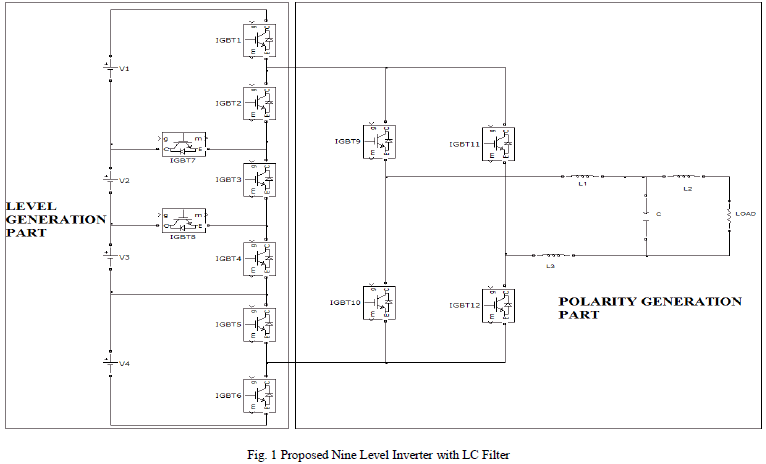 |
| The primary objective of this paper is to minimize the total harmonic distortion of 9-level inverter with an LC filter in the output side. It also minimizes the number of power semiconductor switches than conventional multilevel inverter. For a single-phase nine-level inverter model, there are 16 switches are needed, whereas the proposed model uses only 12 switches. |
MODES OF OPERATION |
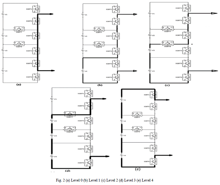
| The operation of this topology can be easily understood by mode of operation of single-phase nine-level inverter shown in Fig. 2. There are nine sufficient switching modes in generating the multistep level for a nine-level inverter. |
 |
| A. Modes of operation |
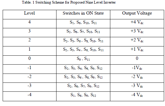
| Operation of the single-phase nine-level inverter with reversing voltage topology can be easily explained with the help of Fig. 2 and Table I |
| 1) Level 0[Fig.2(a)]: The output voltage will be zero (i.e., level 0) when switches S9 and S11 are turned on as shown in Fig. 2(a). |
| 2) Level 1[Fig.2(b)]:The output voltage will be Vdc (i.e., level 1) when switches S2, S3, S4 and S6 are turned on as shown in Fig. 2(b). |
| 3) Level 2[Fig.2(c)]: The output voltage will be 2Vdc (i.e., level 2) when switches S2, S3, S6 and S8 are turned on as shown in Fig. 2(c). |
| 4) Level 3[Fig.2(b)]: The output voltage will be 3Vdc (i.e., level 3) when switches S2, S6, and S7 are turned on as shown in Fig. 2(d). |
| 5) Level 4[Fig.2(c)]: The output voltage will be 4Vdc (i.e., level 4) when switches S1, and S6 are turned on as shown in Fig. 2(e). |
| Switches S9, S10, S11 and S12 are used to reverse the voltage direction when polarity requires to be changed. When switches S10 and S11 are turned on together positive half cycle will be generated and when S9 and S12 are turned on together negative half cycle will be generated across the load. The voltage blocking capacity of each switch is Vdc. Each voltage source Vdc is required 100V. According to the table, there are nine switching combinations to control the multi-level inverter and itshows the great redundancy of the switching devices. Operation of the single-phase nine-level inverter with reversing voltage topology can be easily explained with the help of fig. 2 and Table I |
 |
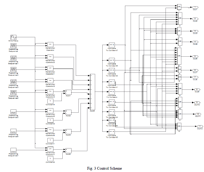
CONTROL SCHEME |
| The control scheme proposed here is a Universal Control Scheme[1] that can be applied for all multilevel inverter topologies and also all the modulation schemes can be incorporated. Thus it takes the advantages of all the existing topologies such as the level-shift (LS) and phase-shift (PS) multicarrier pulse width modulation (PWM), selective harmonic elimination (SHE) etc.For a given inverter, let the number of levels in the phase voltage be NLevel. As said earlier, the term Multilevel began with the three-level converter. That is, NLevel≥ 3. Also, the number of positive levels, |
| N=( NLevel -1)/2 |
| In this control scheme, the modulating signal is always a sinusoidal waveform with amplitude Aref. Also, there should be 2N carrier signals and the waveform of carrier signals is determined by the modulation scheme. Carrier signals will be triangular for sinusoidal PWM and are constants for low frequency schemes like SHE.Carrier signals above the zero reference are designated as f + car,j (t) and those below the zero reference are designated as f – car,j(t). At every instant, each carrier is compared with the modulating signal. For all the carrier signals above the zero reference, each comparison gives ‘1’ if the modulating signal is greater than the carrier signal and ‘0’ if modulating signal is less than carrier signal. For allthe carrier signals below the zero reference, each comparison gives ‘0’ if the modulating signal is greater than the carrier signal and ‘-1’ if modulating signal is less than carrier signal. That is, |
| f + out,j(t)= 1, for fref(t) ≥f + car,j(t) = 0, otherwise |
| f - out,j(t) = 0, for fref(t) ≥ f - car,j(t) = -1, otherwise |
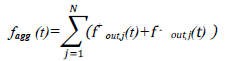
| The result so obtained are added and the signal generated is the aggregate signal, designated as fagg (t), or the aggregate signal, |
 |
| The waveshape of the aggregate signal is same as that of the required output voltage. The driving signal for the semiconductor switches are derived from the aggregate signal using logic circuit and look-up table. |
 |
 |
| To do this, Boolean functions, fd,j(t), are derived from fagg(t) using following criteria: |
| The switching function fswitching(t) , for a given switch, would be obtained by feeding appropriate derived signals into an OR gate. |
| Mathematically, the switching function can be expressed as: |
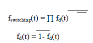 |
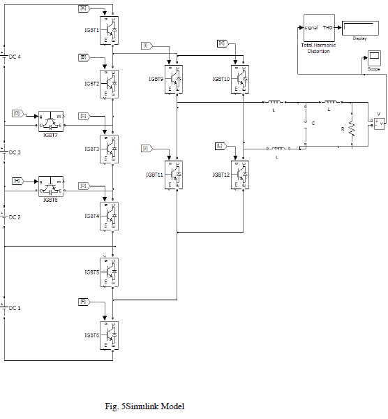
SIMULINK MODEL |
| In this topology, a Universal Control Scheme with Alternate Phase OppositionDisposition multicarrier PWM technique is used. The fig. 4 shows the Simulink model of single-phase nine-level reversing voltage MLI. Twelve IGBTs are used andeach of theswitches requiresa separate gate driver circuit scheme.The output LC filter is used to remove highfrequency switching ripples and is a combination of a 24_F capacitor and a 10-mHinductor. The simulation parameters are as following R = 20 ohms,dcsourcevoltageis50Veach. |
 |
SIMULATION RESULTS |
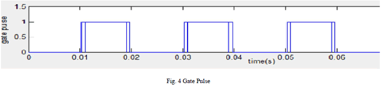
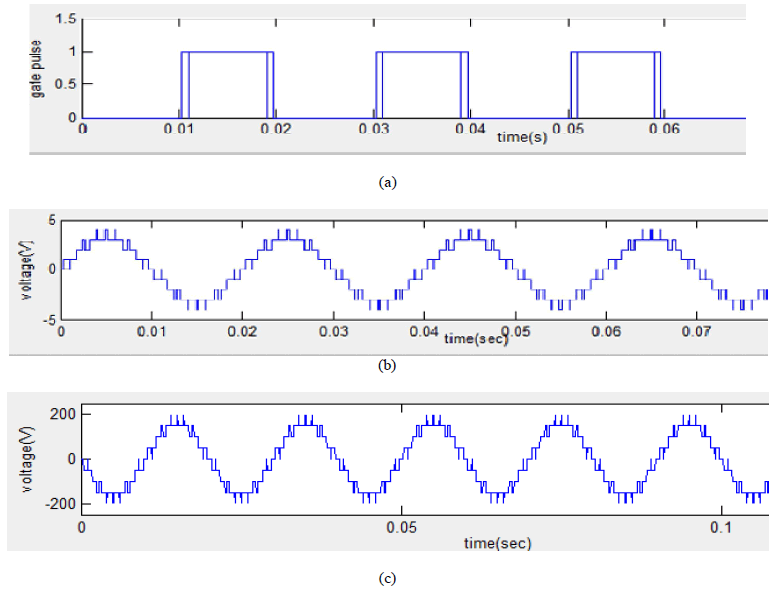
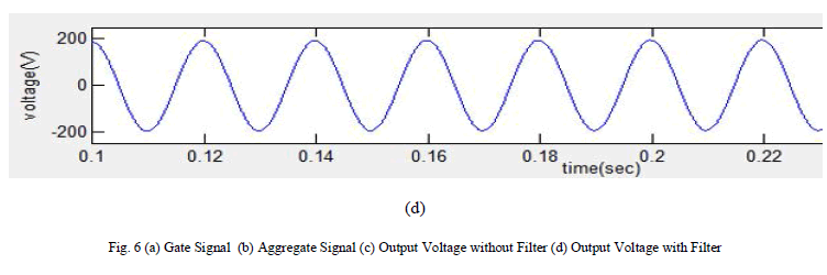
| The proposed Reversing Voltage Nine Level Inverter Topology with Universal Control Scheme was simulated using MATLAB/SIMULINK. Gate pulses were obtained from universal control scheme. The simulation results waveforms are shown. The percent THD was found to be reduced by about 45 percent. The gate pulse for one switch is shown. The gate pulses to the other switches are appropriately phase shifted. The output voltage waveforms and aggregate signals are shown below. |
| The gate pulse to drive the semiconductor switches is shown in fig. 6(a). Gate pulses are derived from the Universal Control Scheme. The aggregate signal which is obtained by comparing the sinusoidal modulating signal and triangular carrier signal is shown in fig. 6(b). The aggregate signal has the same waveshape as that of output waveform. The output voltage waveform without filter is shown in fig. 6(c) and with filter is shown in fig. 6(d). We can infer from the waveform itself that by using a LC filter circuit THD has been reduced significantly and a pure sinusoidal output is obtained. |
 |
 |
CONCLUSION |
| A reversing voltage nine level inverter topology with Universal Control Scheme which compensates for the disadvantages of conventional multilevel inverter is presented in this seminar report. The working, switching function and control scheme has been analysed in this report. The percentage THD for the multilevel inverter with and without filter has been determined and is found to be reduced with the design of LC filter and a sinusoidal output was obtained. The THD was reduced by about 45 percent. Universal Control Scheme was used to drive the inverter. Alternate Phase Opposition Disposition(APOD) Sinusoidal PWM is used. The output waveforms obtained are stepped waveforms. The percent THD was found and and a very small size filter was designed to obtain a percent THD of 0.48 for the ninelevel inverter. |
References |
|