International Journal of Advanced Research in Electrical, Electronics and Instrumentation Engineering
ISSN ONLINE(2278-8875) PRINT (2320-3765)
ISSN ONLINE(2278-8875) PRINT (2320-3765)
| Anjali.R.Prakash PG Student [PEPS], Dept. of EEE, Amal Jyothi college of Engineering, Kottayam, Kerala, India |
| Related article at Pubmed, Scholar Google |
Visit for more related articles at International Journal of Advanced Research in Electrical, Electronics and Instrumentation Engineering
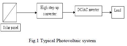
The utilization of photovoltaic energy becomes an important source of electrical energy with the advancement in power electronic technology. The dc-dc converters is one of inevitable part of renewable energy system, for connecting the PV panel to the grid or AC load through an inverter. MPPT (Maximum Power Point Tracking) maximizes the power production of the PV panel. The advantages of high step up converters includes improving voltage gain without using extreme duty ratio, reduction of voltage stress, current ripple and conduction losses are desirable for renewable energy applications. The review of various topologies of high step up converter and their performance with voltage multiplier circuits are discussed in the paper. The merits and demerits of these converters are discussed. This paper shows the comparison of efficiency and voltage gain for various boost converter topologies integration with voltage multiplier
Keywords |
| High step up converter, voltage multiplier, renewable energy, photovoltaic system, high gain |
INTRODUCTION |
| With the development in power electronics technologies the renewable energy sources utilization become an increasing trend for electrical energy. The photovoltaic system is a feasible energy source in research and development work in power system and power electronics. For the better consumption of solar energy a high reliable, low cost, design are required for the PV integrated high step up topologies. High performance dc to dc converter can be obtained with MPPT technique and islanding detection for photovoltaic system are now considered for the interface to the grid or ac utilities [4]. The DC/AC inverters control the output voltage of DC/DC converter and generate a fundamental real power required for the loads. |
| The conventional boost converter provide step up conversion without high gain due the limitation of conduction losses in the circuit parameters. The gain reaches infinite, when the duty cycle tends to unity. The gain depends on the I2R losses in the inductors and the power electronic devices connected. The voltage gain is difficult to obtain with conventional boost topologies because of the parasitic components, which limits the frequency and the system size. A voltage multiplier is a device which converts the low voltage input to a higher voltage by means of capacitors and diodes combined circuit. The voltage multiplier helps in reducing the turns ratio of transformer for better performance. |
| The conventional boost converters are provided with voltage multipliers to increase the voltage gain without having high duty cycle and reduce the voltage stress across the switches. The voltage multiplier reduces the peak current flowing through the switch and enhances the dynamic response with the increase of turn OFF period. |
 |
| DC to DC boost converters are applicable for obtaining regulated value of dc output voltage. The regulation is normally achieved by PWM at constant frequency and the switching device used are usually BJT, MOSFET or IGBT. The high step-up converter helps in improving the voltage gain, reduction of voltage stress and current ripple with optimized circuit performance. The effective circuit component determines the efficiency and gain of the converters used in the photovoltaic system. The integration of voltage multiplier reduces the input current ripple, hence the increases the life of PV arrays of the photovoltaic system. The low voltage output of the PV arrays is stepped up to high voltage for the dc-ac inverter with high efficiency step up converters. Usually the output of the parallel connected PV arrays are low of the range of 30-40V. They are to be stepped up to a value of 380-400V for a full bridge operation, for connecting them to the grid or ac loads [3]. They can also connect directly to dc loads without dc-ac inverter. The various types of high boost converter with their component size and circuit efficiency are discussed in this paper. High efficient loadinteractive PV generation systems with a generation control circuit (GCC) with the photovoltaic cells connecting in series are discussed in [11]. The integration of it with voltage multiplier topologies for better power output is also discussed in the paper. The voltage multiplier aids in increasing the voltage of the boost converter. It consists of diodes and capacitor for charging and discharging of the current to the converter. |
HIGH STEP-UP CONVERTERS WITH VOLTAGE MULTIPLIER |
| The integration of voltage multiplier with high step up converter increases the voltage conversion ratio and gain. The voltage multipliers are provided with capacitors and diodes in the circuit for converting the input voltage to another high level output [10]. The converter with the voltage multiplier determines the efficiency and performance of the photovoltaic system connected to the system. |
A. Interleaved high step up converter with voltage multiplier |
| In high power applications, the interleaving improves the performance and reduces the size of the boost converters required. The interleaved step up converter has ZCS switching by the leakage inductance of coupled inductors [3]. The leakage energy can be reused by the clamp capacitor and the diode and reduces the voltage spikes at the output. The advantage of using interleaved structure is that the converter can be used for high power application in the photovoltaic system. |
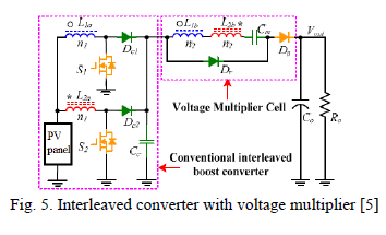 |
| The voltage multiplier circuits are provided in the system to improve the gain and reduce the voltage stresses reduced across the switches. The interleaved converters reduce the current and voltage stress, with the reduction in size of inductors and capacitors used. The addition of snubber circuit in the circuit increases the conduction losses by the diode reverse recovery current. The problem can be resolved by the use of three state switching cell with voltage multiplier. |
| The disadvantage of using these interleaving are high rms current and high ringing of voltage at the switch due to the capacitor ESL. The diode reverse recovery affects the overall efficiency of the converter. |
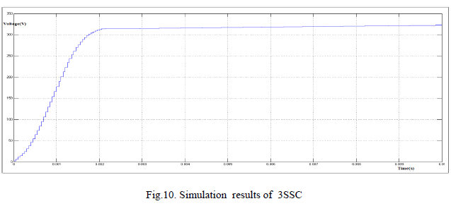
A. DC-DC converter with 3SSC and VMC |
| The three state switching cell are incorporated with the voltage multiplier for improving the gain. The advantage of using this topology of converter is the reduced number of components, weight and volume of the circuit. The current flowing through the switch is same as the output current. The energy flow is from source to the load during the switching period. The advantage of this topology is low current ripple and voltage stress. The output of the system can be improved by adjusting the turns ratio of transformer used. The three state switching cells are used to reduce the winding size of the converter. The performance of the converter is high for all the value of input voltages. This reduces the transformer saturation problem and conduction losses by the leakage inductances. |
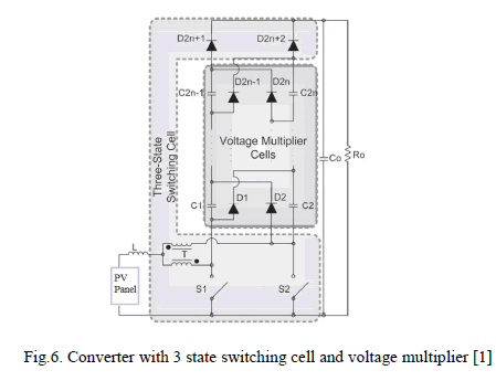 |
| The limitation of the converter is the complex drive circuit requirement. Small snubber circuits are provided in the circuit for each switch. The circuits are provided with hard commutation. The voltage multiplier are working at d>dmin. |
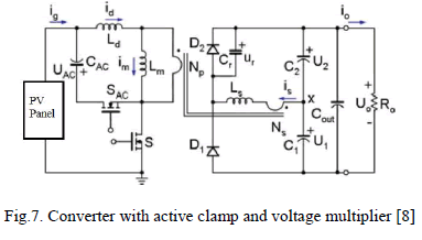
B. DC-DC converter with active clamp and voltage multiplier |
| This converter employs a transformer with primary side having clamp and secondary with voltage multiplier. The active clamp circuits helps in high voltage conversion and are used in ON and OFF state of the converter for delivering power. The diodes parasitic capacitance reduces the conduction losses with decrease in circulating current on active clamp circuit during the turn off of the main switch. |
| The disadvantages are the balance in voltage due to output capacitors. With the resonant operation the switches are turned ON at hard switching and turned OFF at soft switching. The snubber circuits at the output are required to reduce the voltage across the switch. |
 |
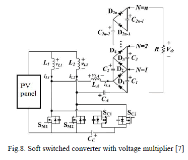
C. High step-up soft-switched converters using voltage multiplier cell |
| These converters are provided for the double voltage conversion. The Zero voltage switching (ZVS) turn ON are provided for the switch and ZCS (Zero current switching) turn off the diodes in the circuitry. The converter consists of clamp switch, main switch, voltage multiplier cells, inductor switch legs. The duty cycle of the clamp switch can be varied from 0 to 1. The main switch is turned OFF by hard switching. With the duty cycle greater than 0.5 the losses in the circuit are reduced. Hence reduces the reverse recovery problem due to switches and low rated switches can be used in the converter for the main and clamp switches. The advantages of this topology of high step up converter are the low current ripple and increasing flexibility. The voltage spikes due to the parasitic components at the output are clamped. |
 |
D. Cross coupled inductor and voltage multiplier |
| This converter works with zero cross switching (ZCS) turn on soft switching. The leakage energy is recycled, hence the diode reverse recovery is reduced. This improves the gain and the reduces the voltage stress across the switch. The conduction losses are reduces with the reduction of voltage stress and increase in turns ratio of coupled inductors [6]. The voltage across the switch is half of the output voltage. Low power MOSFET reduces the problems due to conduction losses drastically, and reduces the size of semiconductor devices used. The winding cross coupled inductors (WCCI) are used for high step up conversion of the system. |
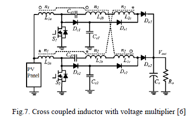 |
| The limitation is that the duty cycle should exceed 0.5 with the steady operational analysis. The three windings in WCCI make the circuit complex and difficult for industrial manufacturing. |
E. Cockcroft Walton voltage multiplier |
| Cockcroft Walton (CW) voltage multipliers are used in application where high gain required. The circuit consists of inductor, switches, n-stage voltage multipliers. One of the diode in CW conducts when the inductor transfers energy to the circuit. The voltage across the output is equal to the voltages across the capacitors at the bottom. |
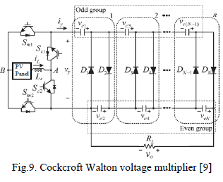 |
| The voltage stresses in the diodes are twice than that of the switches. They operate in continuous conduction mode. The advantages are the four switches are operating at two different frequencies. The dc outputs from capacitors are suitable for powering multilevel inverters. The limitations of the topology are the complexity and cost to drive the power semiconductor switches. |
SIMULATION RESULTS |
 |
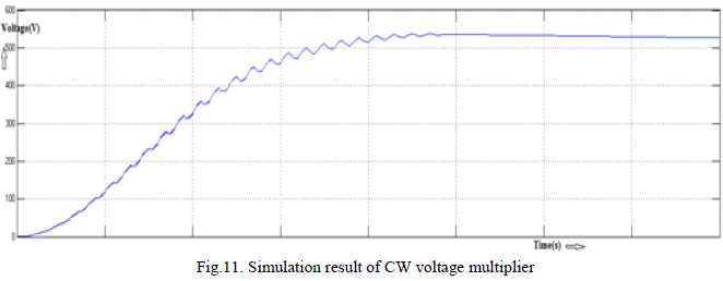 |
| The figures 10 and 11 shows the simulation results obtained with the comparison of converters. The gain for CW voltage multiplier is more compared to other converters. |
CONCLUSION |
| The comparison of various high step up converter with voltage multiplier with their efficiency and voltage gain equations are discussed in the Table 1. The gain of the converter depends on the design, components used in the topology. The maximum power can be tracked in the photovoltaic system for better performance. The design of the converter determines the performance of the system. The smaller value of duty cycle increases the robust working of the photovoltaic system. The different methods are applicable for various application such as reduction in conduction losses, voltage stress across the switch, leakage energy recycling, better efficiency and gain. The voltage multiplier cells integrating the circuit reduce input and current ripple and the stress in the switches. |
References |
|