International Journal of Advanced Research in Electrical, Electronics and Instrumentation Engineering
ISSN ONLINE(2278-8875) PRINT (2320-3765)
ISSN ONLINE(2278-8875) PRINT (2320-3765)
Deepak Kumar1, K.Anusudha2
|
| Related article at Pubmed, Scholar Google |
Visit for more related articles at International Journal of Advanced Research in Electrical, Electronics and Instrumentation Engineering
This paper presents the Reduced Instruction Set Computer (RISC) system using VHDL and the results are analyzed in an FPGA system . This paper presents a RISC processor designing to achieve OR, AND, NAND, NOR, XOR, XNOR, ADD, SUBTRACT, NOT, INCREMENT, DECREMENT, etc operations. The 20-bit RISC system has high general-purpose register (GPR) orthogonality and communicates to peripheral devices via a serial bus.
Keywords |
| Arithmetic Logic Unit (ALU), Control Unit (CU), General Purpose Register(GPR), Program Counter(PC) Instruction Register(IR), Reduced Instruction Set Computer(RISC) . |
INTRODUCTION |
| RISC-The IBM was the first company to define the RISC (Reduced Instruction Set Computer) architecture in the 1970s. This research was further developed by the universities of Berkeley and Stanford to give basic architectural models. |
| RISC can be described as a philosophy with three basic levels: |
| All instruction will be executed in a single cycle. |
| Memory will only be accessed via load and store instruction. |
| All executions units will be hardwired with no micro coding. |
| Reduced Instruction Set Computer (RISC) strategy based on the insight that simplified instructions can provide higher performance if this simplicity enables much faster execution of each instruction. It use fewer instructions with simple constructs, therefore they can be executed much faster within the CPU without having to use memory as often.[2] |
| The instruction set is the hardware âÃâ¬Ãâ¢language in which the software tells the processor what to do. Surprisingly, reducing the size of instruction set, eliminating certain instructions based upon a careful quantitative analysis, and requiring these seldom, used instructions to be emulated in software can lead to higher performance. For several reasons Some of the uses for the space: |
| Additional registers. |
| On-chip caches which are clocked as fast as the Processor. |
| Additional functional units for superscalar execution. |
| Increased pipeline depth. |
| Branch prediction. |
| The vacated area of chip can be used in ways that accelerate the performance of more commonly used instructions. |
| It becomes easier to optimize the design. |
| It is a type of microprocessor architecture that utilizes a small, highly-optimized set of instructions. It is designed to perform a smaller number of types of computer instructions so that it can operate at a higher speed. |
| Main features of a RISC processor are to load/store designs few addressing modes, fixed instruction size, few instruction formats, few operand sizes, use more registers, separate memory operations, better compilation, many instructions that access memory directly, variable length instruction encoding and pipelining can be implemented easily. [5] |
| Basically the philosophy is that instructions are handled in parts: |
| Fetch the instruction. |
| Get the arguments |
| Perform the action |
| Write back the result |
| It has the ability to execute one instruction per cycle. This is done by overlapping the fetch, decode, and execute phases of two or three instructions by using a procedure referred to as pipelining. The RISC provides higher performance in computing because of little need of the external fetches, which take significant amount of processor time and also because of hard-wired instruction implementation [5]. |
| FPGA- Field Programmable Gate Array. Conceptually it can be considered as an array of Configurable Logic Blocks (CLBs) that can be connected together through a vast inter connection matrix to form complex digital circuits. It is an integrated circuit designed to be configured by a customer or a designer after manufacturing—hence "fieldprogrammable". The FPGA configuration is generally specified using a hardware description language (HDL). FPGAs contain programmable logic components called "logic blocks", and a hierarchy of reconfigurable interconnects that allow the blocks to be "wired together"—somewhat like many logic gates that can be inter-wired in different configurations.[6] |
| Main features of FPGA are- |
| Simple’ Programmable Logic Blocks. |
| Innovative logic structure. |
| Larger Logic Functions built up by connecting many Logic Blocks together. |
| Massive Fabric of Programmable Interconnects. |
| Rich feature set including high-performance DSP blocks and on-chip memories. |
| FPGAs are perfect for rapid prototyping of digital circuits |
| High speed I/O pins and external memory interfaces. |
| CLBs – It stands for configurable logic blocks. It provides the functional element to implement most of the logic gates. |
| Input/output Blocks – It provides the interfacing between the package pins and the internal logic. |
| Delay–Locked loops (DLLs) – It is used to distribute the clock and properly compensate the delays. |
| Blocked RAMs – Each RAM has 4096 bits. |
| The paper is organised in such a way that the section II explains the Proposed Risc Architecture, section III explain the instruction format , section VI explain the instruction set; section VII shows the simulation results for different inputs. Finally, section VIII summarises the paper. |
PROPOSED RISC ARCHITECTURE |
| The Architecture of RISC system is shown in Fig. 1. It includes Memory, Instruction Cache, Data Cache, Standard Processor and Configurable array. |
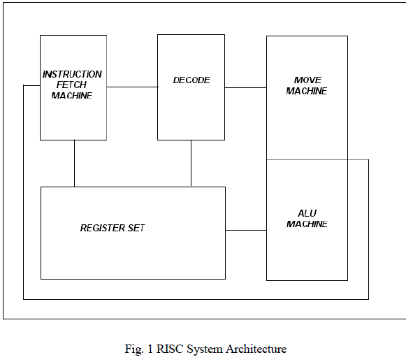 |
| RISC consists of: This system can be separated into several states as shown in Figure 1. Each state describes the current operation or process being performed by the CPU and is described in a VHDL module. Each module is connected via a single high-level module. The high level module is displayed in Figure1. This system is the hardware within a computer system which carries out the instructions of a computer program by performing the basic arithmetical, logical, and input/output operations of the system. |
| Register Set (RS): In this information is encoded, stored, and retrieved. The RS of this system contains the following registers: |
| ïÃâ÷ IR - holds the current instruction. |
| ïÃâ÷ PC - holds the address of the next instruction. |
| ïÃâ÷ Load - holds data loaded from memory. |
| ïÃâ÷ Store - holds data being stored to memory. |
| ïÃâ÷ SR - when an operation involves two operands, the status signals are updated. The SR can also the used as an operand in arithmetic and logical operations. |
| ïÃâ÷ GPR[x] -up to 64 GPRs can be used in this architecture. |
| All GPRs and the SR can be used in any operation except for the load and store instructions. Only GPR can be used for loading and storing. |
| Instruction Fetch Machine: This machine fetches an instruction from external memory, and upon completion of the instruction fetch cycle this machine signals the decoder to decode the instruction. This machine utilizes a 3-bit upcounter with an active low reset. the CPU changes states and begins to decode the instruction. |
| Decoder: Upon completion of the instruction fetch cycle, the instruction is decoded. The decoder reads bit 3 down to 0 of the IR, decides which of the sixteen operations the CPU needs to performs, and signals one of the next states to begin its operation. |
| Move Machine: The move machine controls all register movement. The most basic of these movements is the movement of data from one GPR to another GPR.Upon completion of the movement of data, a new instruction is fetched. |
| Arithmetic Logic Unit: The ALU performs arithmetic and logical operations on data. The data is taken from two GPRs and is moved to the ALU. The result is stored in a GPR. For operations that involve one operand, a GPR can be specified to store the result. The ALU supports two’s complement data. |
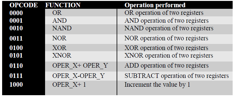
INSTRUCTION SETS |
| The processor with 4 bit opcode to allow instruction to perform various operations such as or ,and , nand, nor , xor, xnor , add , subtract, not , increment, decrement, etc. Each opcode has specific operation in processor; RISC have 4-bit opcode that can perform 16 different operations. Table 2 shows the instruction set for RISC processor. |
TABLE II |
| INSTRUCTION SETS |
 |
INSTRUCTION FORMAT |
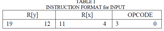
| The RISC is 20-bit processor so that the value of each instruction is 20 bits. Each instruction decodes by internal decoder and RISC machine fetches an instruction from the memory. In this RISC two 8-bit instructions are coming as inputs i.e. 8-bit x and 8-bit y. and 0 to 3 bits is the opcode for instruction of performed operations. Table no.1 shown the input instruction format.[5] |
 |
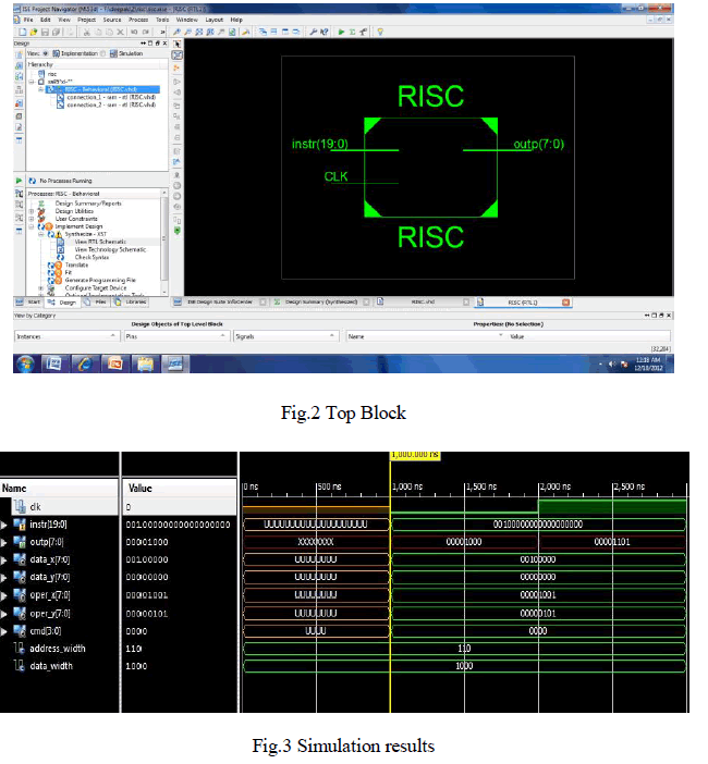
SIMULATION & RESULT |
| The RISC processor is simulated using Xilinx ISE version 13.2. The simulation result is shown in Figures. Top Block of RISC is shown in fig. 2; Simulate Behavioral Model shown in Fig. 3; simulation with test bench for all opcode shown in fig.4; output for OR Gate, AND Gate and NAND gate shown in fig.5; output for NOR Gate, XOR Gate and XNOR gate shown in fig.6; output for ADD operation and SUBTRACT operation shown in fig.7. |
 |
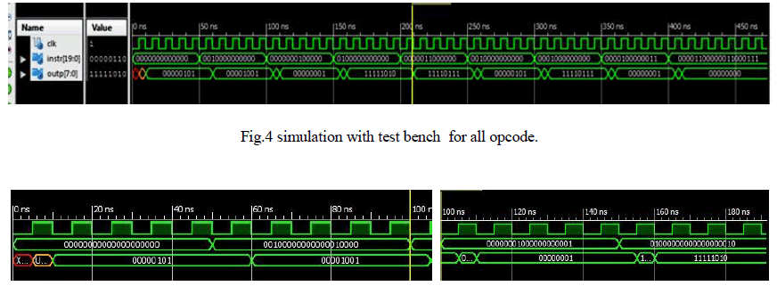 |
| The value of oper_x is 00100000 and data_x is 00000000; Oper_y is 00000000 and data_y is 00001001, the instruction for 0000 is Or, for OR operation the output result is 00001001. |
| The value of oper_x is 00100000 and data_x is 00001001; Oper_y is 00000000 and data_y is 00000101, the instruction for 0001 is AND, for AND operation the output result is 00000001. |
| The value of oper_x is 01000000 and data_x is 00000101; Oper_y is 00000000 and data_y is 00000101,the instruction for 0010 is NAND, for NAND operation the output result is 11111010. |
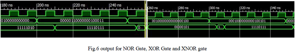 |
| The value of oper_x is 00000110 and data_x is 00000000; Oper_y is 00000010 and data_y is 00001000,the instruction for 0011 is NOR, for NOR operation the output result is 11110111. |
| The value of oper_x is 00100000 and data_x is 00000000; Oper_y is 00000010 and data_y is 00000101,the instruction for 0100 is XOR, for XOR operation the output result is 00000101. |
| The value of oper_x is 00010000 and data_x is 00000000; Oper_y is 00000010 and data_y is 00001000,the instruction for 0101 is XNOR, for XNOR operation the output result is 11110111. |
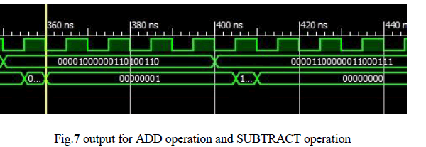 |
| The value of oper_x is 00001000 and data_x is 00000000; Oper_y is 00011010 and data_y is 00000001,the instruction for 0110 is x+y, for x+y operation the output result is 00000001. |
| The value of oper_x is 00001100 and data_x is 00000000; Oper_y is 00001100 and data_y is 00000000,the instruction for 0110 is x-y, for x+y operation the output result is 00000000.CONCLUSION |
CONCLUSION |
| The design has been implemented and easily seen in the Xilinx ISE Design Suite 13.2 window as waveform. Processor has been designed and implemented in hardware on Xilinx Spartan 2E FPGA. The design has been achieved using VHDL and simulated with ModelSim. Digilent Spartan 2E development board has been used for the hardware part. This paper has presented a small and easy to understand processor developed using VHDL. It executes all the instructions in one clock cycle, including jumps, returns from subroutines and external accesses. The assembler of this processor is full of macros that extend the native instruction set to facilitate low level programming. |
References |
|