International Journal of Advanced Research in Electrical, Electronics and Instrumentation Engineering
ISSN ONLINE(2278-8875) PRINT (2320-3765)
ISSN ONLINE(2278-8875) PRINT (2320-3765)
P.Mohan1, Dr.V.Balaji2, G.S.Sugnaya1
|
| Related article at Pubmed, Scholar Google |
Visit for more related articles at International Journal of Advanced Research in Electrical, Electronics and Instrumentation Engineering
A new self-synchronous bi-directional converter for Electrical Vehicle (EV) charging system is described. The circuit uses bridgeless boost operation while rectifying and split DC feeding while inverting. Automatic synchronization is achieved by generating the gating signals from the ac grid.
Keywords |
| Bi-directional converter, MOSFET switches Bridgeless boost operation,V2G, self-synchronizing inverter. |
INTRODUCTION |
| In Vehicle to Grid (V2G) scheme [1] [2], the DC energy stored in the batteries of Electric Vehicles (EVs) is delivered back to the AC grid depending on the availability of DC energy and needs of the grid. The converters used in a charging station provide this bidirectional energy transfer service. |
| Several converter topologies are available for V2G operation. While delivering AC power to the grid, synchronization of the local inverter AC output with that of the grid is an important requirement. Both frequency and phase angle should match. In our proposed scheme, we provide a simple mechanism for self-synchronization. Rectification operation can be realized in many ways. we use two bridgeless boost rectifiers to generate a dual DC power source which help us in the converter design. Bridgeless boost rectification provides low loss and less ripples. |
BASIC CIRCUIT |
| The basic circuit is shown in Fig.1. It is a dual rectifier single inverter configuration. |
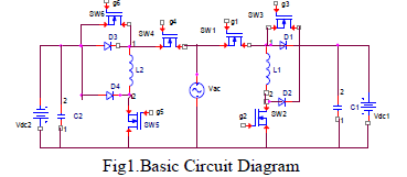 |
| In Fig. 1, the rectifier operation on the right side generates VDC1 and that on the left side generates VDC2. |
| Bidirectional four quadrant switches |
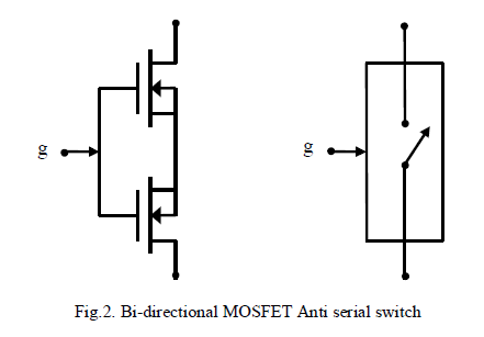
| SW1, SW2,…SW6 are the MOSFET Bi-directional switches as shown in Fig.2. A bi-directional four quadrant switch is realized by the anti serial connection of two MOSFETS. The on-off state of the switch is controlled by the gate control signal. When the gate signal g goes high (logic 1), the switch closes and when the gate signal goes low (logic 0), the switch opens. |
 |
| Operation as Rectifiers |
| The right hand side of the circuit in Fig.1, acts as a bridgeless boost rectifier when SW3 is kept off throughout and SW1, SW2 are controlled properly as described in [5]. The charging current, voltage and power can be controlled according to the requirement. Similarly, when SW6 is kept off throughout, the left hand side of the circuit acts as a bridgeless boost rectifier. The control scheme for the left side is similar to that on the right side. Thus SW3 and SW6 do not participate in controlling the rectifier operation. The details are given in [5]. |
OPERATION AS AN INVERTER |
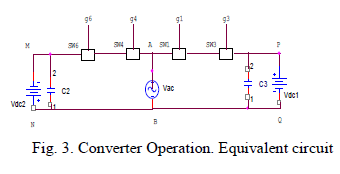
| During inverter operation, SW2 and SW5 are kept completely turned off. The diodes D1, D2, D3 and D4 remain off during inverter operation. Because of this, L1 and L2 will not play any role during converter action. The equivalent circuit during inverter operation is shown in Fig. 3. |
 |
| Passive load across AB |
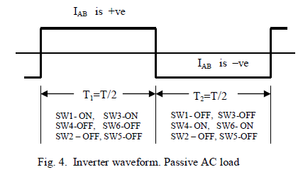
| For the purpose of basic understanding of the circuit, let us assume a passive resistive load RAB across AB. During a time interval T1, turn on SW1, SW3 and turn off SW4, SW6. Now the current flows through P_SW3_SW1_A_RAB_B_Q_P. The ac current flows from A to B. The DC source VDC1 drives the current through RAB.. During the next time interval T2, turn off SW1, SW2 and turn on SW4, SW6. Now the current flows through N_B_RBA_A_SW4_SW6_M_N. The ac current flows from B to A. The DC source VDC2 drives the current through RAB. During T1, IAB is +ve and during T2, IAB is –ve. By making T1 = T2 = T/2, the two half cycles are made equal. By taking âÃâÃâVDC1âÃâÃâ equal to âÃâÃâVDC2âÃâÃâ, the magnitudes f the currents in two halves are made equal. the current waveform is shown in Fig.4. Since , T1 = T2 = T/2, the period is T and the frequency is f=1/T. |
 |
Sine wave AC |
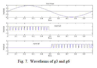
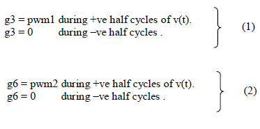
| The output AC voltage/current is made almost sinusoidal, by using PWM switching of SW3 during +ve half cycles and PWM switching of SW6 during –ve half cycles. Note that SW3 and SW6 are not used for control operations in rectifier mode. Hence they are used now, in the inverter mode. |
| In switched mode inverters, PWM waves are used to shape the wave form. To generate a sine wave output, the PWM signal is generated by comparing a triangular wave with a reference sine wave as shown in Fig. 5. |
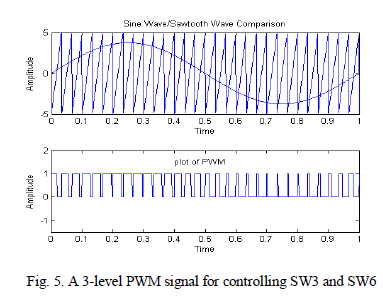 |
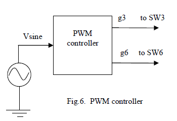
| Basically a triangular wave of high switching frequency is compared with a reference sine wave using a comparator to generate the PWM output. The switching frequency is chosen appropriately. The frequency and phase angle of the inverted output is controlled by the reference sine wave input designated as Vsine. A schematic block diagram of a PWM controller is shown in Fig.6. The triangular wave is generated internally. The user can choose the switching frequency. SW1 and SW4 are kept on throughout during inverter operation. |
 |
| The PWM switch control signals g3 and g6 will be as shown in Fig. 7. Signal g3 is active during +ve half cycles of AC and signal g6 is active during –ve half cycles. During –ve half cycles, g3 = 0. This keeps SG3 OFF during that period. Similarly g6=0 during +ve half cycles keeps SG6 OFF. In actual practice g3 and g6 should pass through standard MOSFET gate drivers like IR 2304’s, IR2110(S), etc. The PWM controller is realized using IC’s like TL494, UCC1829. |
 |
SIMULINK MODEL FOR THE INVERTER OPERATION |
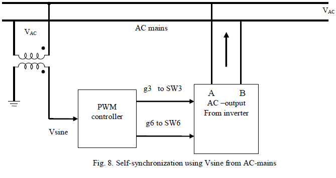
| A simplified simulink model of the inverter operation with a passive load, is shown in Fig. 9. The reference sine wave input v(t) (same as Vsine) to the PWM generator is a 1 volt 50 Hz sine wave. |
| PWM generator produces two pulse trains pwm1 and pwm2. The waveform of pwm1 will be as shown in Fig. 5. The waveform of pwm2 is the complement of pwm1. Our requirement is pwm1 should drive SW3 during +ve half cycles and pwm2 should drive SW6 during –ve half cycles of AC. Another important condition is, SW3 should be OFF during –ve half cycles and SW6 should be OFF during +ve half cycles. This means, |
 |
| In Fig. 9, signals g3 and g6 are generated using the sign function as follows. First, we get y=sign(v(t)). Signal y is +1 during +ve half cycles and –1 during –ve half cycles. Then we get signals u1 and u2 as, |
 |
| From the definition of sign(v(t)) and Eq. (3), we get |
| u1 = 1 when v(t)>0, that is, during +ve half cycles of v(t). |
| u1 = 0 when v(t)<0, that is, during –ve half cycles of v(t). |
| Similarly, |
| u2 = 0 when v(t)>0, that is, during +ve half cycles of v(t). |
| u2 = 1 when v(t)<0, that is, during –ve half cycles of v(t). |
| Now we realize g3 and g6 as, |
| g3 = pwm1*u1 (5) |
| g6 = pwm2*u2 (6) |
| The resulting g3 and g4, from the product operations of Eqs. (5) and (6) satisfy the conditions of Eqs. (1) and (2). The AC output is taken through an output transformer so that any desirable output voltage magnitude can be selected. An LC filter with 1 micro-Farad capacitor and an 150 mH inductors is used to remove the switching noise. |
INVERTER FEEDING THE AC GRID |
| In this case, the inverter output is connected to the AC grid. Now the frequency and phase angle of the inverter output should exactly match that of the grid AC voltage. That is, we have to synchronize the inverter output with the grid AC system. |
Self-Synchronization |
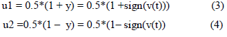
| In our proposed circuit, synchronization is achieved by getting the PWM controller reference input Vsine (see Fig. 6) from the grid AC line itself as shown in Fig. 8. A step down transformer supplies Vsine from VAC. The output from AB terminals of the converter is fed into the grid system after proper filtering and voltage level adjustment. |
 |
 |
 |
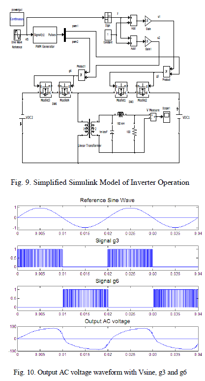
| The AC output voltage waveform along with reference sine wave input, g3 and g6 are shown in Fig.10. The output waveform is distorted because of the LC filter. The noise level and distortion in the output depends on the LCfilter values, switching frequency and the AC load resistance. |
CONCLUSION |
| A new bi-directional converter is proposed. It uses two DC sources and 6 bi-directional MOSFET switches. Because of dual DC sources, realization of the inverter becomes cost effective. The inverter operation is automatically synchronized to the AC grid. This will be very useful for Plug in EV’s battery charging systems. The V2G operation can be easily achieved using the self-synchronizing inverter operation. The circuit is scalable and can be easily adopted for poly phase operation. |
References |
|