International Journal of Advanced Research in Electrical, Electronics and Instrumentation Engineering
ISSN ONLINE(2278-8875) PRINT (2320-3765)
ISSN ONLINE(2278-8875) PRINT (2320-3765)
Harshil Shah1
|
| Related article at Pubmed, Scholar Google |
Visit for more related articles at International Journal of Advanced Research in Electrical, Electronics and Instrumentation Engineering
These topic illuminates to develop the protection system for high power inverters using Microcontroller.. The current system consist of IGBT for the high power inverters and according to the simulation results hardware implementation is done with controller board. For the reference values for Microcontroller code generation, one power circuit can be developed .Power circuit with controller will work in such a way that if any fault occurs in the system then the system will be protected. controller board can be interface with the hardware and in software of DSP program can be developed for the feedback of the protection system. According to the simulation results hardware implementation can be done.
Keywords |
| Peak Voltage, microcontroller, voltage across IGBT, Conducting Current, Peak Amplitude, Power Factor. |
INTRODUCTION |
| Basically in this high power inverter module, voltage level should be maintained so that other fault level can be decreased. According to parallel load connection, inverter gate drive circuits will change pulse for the thyrister. |
| We can simulate this inverter circuit in single phase and three phase also. In controller section DSP is used so that perticuler limit for the peak value should be decided and according to that if fault goes above or below that limit the whole circuit will open so that components used in the circuit will be safe and protection of circuit can be easilly developed. |
| Without use of snubber circuit, spikes in the voltage and distortion in the current waveforms can clearly notify and that can be minimized only by adding snubber circuit. Sharing resister are also to be added in the circuit for the balancing of voltage levels. Voltage monitoring and digital control system can be used also but microcontroller is more user friendly than all other controller systems in recent days. |
| The main outcome of this topology is to develop the protection system in such a way that the semiconductor device like IGBT will be protected if any fault occurs during high power mode because for particular high power mode there is more IGBT required to distribute the voltage stress across the switches. If more number of switches is there than the system should work properly and if fault occurs and somehow any IGBT is not able to handle power flow than it will affect the system consistency and output voltage result. |
| And basically with inter phasing of Microcontroller according to the application demand, programming is done to design the system for protective purpose. Change in microcontroller parameter will occur the change in the system according to the requirement. Main concept of protection of high power during running condition is being satisfied with inter phasing of microcontroller. |
II.PROPOSED MODEL AND ASSUMPTIONS |
| Programming and code generation in the microcontroller is according to the fault level and other parameters which are being changed during fault according to the system. |
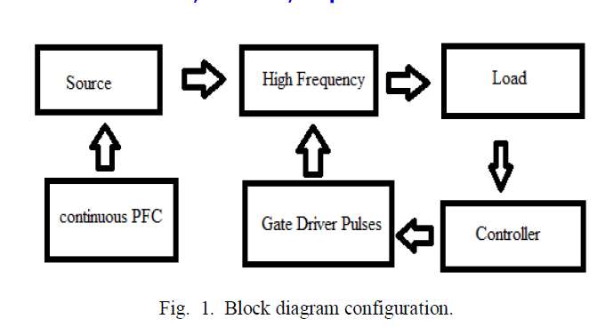 |
| Basically in this module block power is being transferred towards semiconductor devices according with proper frequency and here IGBT is being taken as a semiconductor switch and results are being obtained on the basis of the IGBT results. Load is connected towards the circuit and controller is interface with circuit to provide gate driver pulses to the IGBT gate terminal and continuous PFC is there to maintain the source. |
| DSP controller consist of ADC, DAC, Buffer and some other ports are there for the analysis of the protection system for high power inverters. The voltage waveform across the thyristor and here in this system in single phase four thyristor are connected in one lag, it means two IGBT are in series in one lag so during positive half cycle four thyristor will conduct and negative half cycle other four IGBT will conduct in single phase system. Here the same voltage across thyristor waveforms we can get in hardware also which can be taken as a reference for the controller section. If we are using two IGBTS are in series then the results of that two thyristor will be almost same because they are blocking same voltage but the voltage will get divide so as many IGBT used in a system we can say that the voltage will get balanced, so the load or stresses on each IGBT will get reduced. |
| So according to the simulation and hardware results are being observed on simulation basis also and according to microcontroller bases. By varying the parameters current and output voltage waveforms can also be varied. |
III.SIMULATION RESULTS |
| Here basically in simulation results various types of topology results are being observed and according to that results hardware description is done and the performance of IGBT is being observed by the simulation based results so that protective system can done by controller interfacing. |
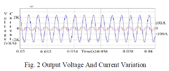 |
| here in Fig.2 Voltage and Current variations are being observed as load changes and in Fig .3 Voltage results of the DSP controller final is obtained here basically result is required like shown in Fig.3 because controller will fix one limit on the peak side so that any fault occurs in the system can minimized and system can be protected. |
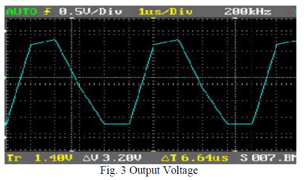 |
| Here in Fig. 3, It is shown that the output voltage is observed as the microcontroller inter phasing results and the value according to the voltage demand is satisfied to protect the high power inverters. |
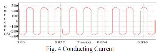 |
| Here in Fig. 4, the result of the conducting current is shown which is around 250A is there for high power module according to the mains changes the output results also changes. |
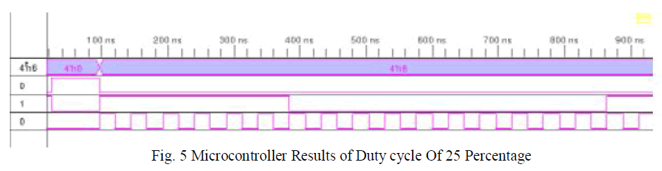 |
| Here in Fig. 5, According to the programming in the microcontroller, Duty cycle for various percentage is observed for the results and here the duty cycle of 25% is shown. |
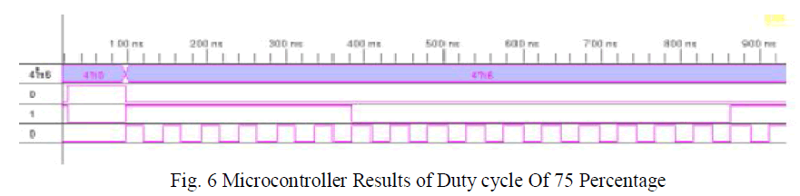 |
| Here in Fig. 6, microcontroller results the duty cycle of 75% for the output parameters variation and this is required for the IGBT gate driver pulses as for instant response and to satisfy the concept to protect the inverter of high power module basically in the system. |
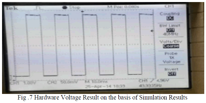 |
| Here in Fig.7 Hardware results are being obtained as same as the simulation results to develop protective based systems. |
IV.CONCLUSION |
| Here from this concept we can conclude that protection system for the high power inverters can be implemented by sensing the voltage across thyristor, snubber voltage and current waveforms in Controller and according to that result hardware system is also being implemented. |
ACKNOWLEDGMENT |
| The authors gratefully acknowledge the support of the Electrotherm India, Ahmedabad in the development of the system and also the support of the Nirma University Ahmedabad for platform. |
References |
|