International Journal of Advanced Research in Electrical, Electronics and Instrumentation Engineering
ISSN ONLINE(2278-8875) PRINT (2320-3765)
ISSN ONLINE(2278-8875) PRINT (2320-3765)
K. Manikandan1, N.Karthick2
|
| Related article at Pubmed, Scholar Google |
Visit for more related articles at International Journal of Advanced Research in Electrical, Electronics and Instrumentation Engineering
An electrolytic capacitors used as a decoupling reservoir which restrict the lifetime of photovoltaic (PV) micro inverters. This has led to the development of several improved decoupling circuits that can reduce the capacitor value to allow the use of non electrolytic types. The project focus on selection of the minimum decoupling capacitor value for the proper operation of discontinuous conduction mode fly back PV micro inverters by considering the total harmonic distortion (THD) and PV power utilization ratio. A decoupling capacitor selection method for single-stage and two-stage fly back inverters is proposed. The results presented show that the decoupling capacitor value influences the THD more than PV power utilization. For single-stage inverters, the decoupling capacitor is placed across the PV output terminals, and should be sized according to the desired THD limit instead of PV power utilization. For two-stage inverters, the control method of the dc–dc converter determines the stage where the decoupling function takes place. Thus, the PV side decoupling capacitor should be dimensioned according to the PV power utilization ratio, and the inverter side decoupling capacitor should be selected according to the desired THD limitation. The corresponding voltage ripple limits for THD and PV power utilization ratio satisfy the IEC standard values of 5% and 9.6%, respectively.
Keywords |
| Flyback photo voltaic micro-inverters Decoupling capacitors, Total Harmonic Distortion, and photo voltaic power utilization |
INTRODUCTION |
| Solar power is the generation of electricity from sunlight. This can be direct as with photovoltaic’s (PV), or Indirect as with Concentrating Solar Power (CSP). Photo voltaics (PVs) are arrays of cells containing a solar photovoltaic material that converts solar radiation into direct current electricity. Materials presently used for photovoltaic include monocrystallinesilicon, polycrystalline silicon, amorphous silicon, cadmium telluride, and copper indium selenide/sulfide. The micro inverter is a single compact unit that converts the DC power from the solar module to AC power for supply to the electricity grid without the need for string or central inverter. The AC output from the micro inverter is in phase with the electricity grid and exhibits high power quality including low harmonic distortion and unity power factor. A micro inverter is a miniaturized voltage converter attached to the back of solar panels. In conventional solar PV systems, panels are strung together in a series, all linked to one centralized power inverter. One drawback of this approach is system-wide failure. A decoupling capacitor is a capacitor used to decouple one part of an electrical network (circuit) from another. Noise caused by other circuit elements is shunted through the capacitor, reducing the effect it has on the rest of the circuit. Decoupling capacitors are used to reduce unwanted AC signals riding on DC supply circuits. It places in a circuit where AC signals need to be eliminated. These are usually placed between the DC supply and the ground of the circuit or directly across another component. The capacitors effectively maintain powersupply voltage at frequencies from hundreds of kHz to hundreds of MHz (in the milliseconds to nanoseconds range). |
| The aim of the project is to carry out the Electrolytic capacitors as a decoupling reservoir which restrict the lifetime of photovoltaic (PV) micro inverters. This has led to the development of several improved decoupling circuits that can reduce the capacitor value to allow the use of non electrolytic types. In this project, the minimum decoupling capacitor value for the proper operation of discontinuous conduction mode fly back PV micro inverters is analyzed by taking into account the total harmonic distortion (THD) and PV power utilization ratio. The results presented show that the decoupling capacitor value influences the THD more than PV power utilization. A decoupling capacitor selection method for single-stage and two-stage fly back inverters is proposed. |
RELATED WORK |
| The review paper [18], focuses on inverter technologies for connecting photovoltaic (PV) modules to a single-phase grid .The inverters are categorized into four classifications: 1) the number of power processing stages in cascade; 2) the type of power decoupling between the PV module(s) and the single-phase grid; 3) whether they utilizes a transformer (either line or high frequency) or not; and 4) the type of grid-connected power stage. |
| In [24] a Future Renewable Electric Energy Delivery and Management (FREEDM) system which provides a DC interface for alternative energy sources is proposed. |
| In [24], a high-efficiency dual mode resonant converter topology is proposed for parallel connected dc MICs. This new resonant converter topology can change resonant modes adaptively depending on the panel operation conditions. This study explains the operation principle of the proposed converter and presents a dc gain analysis based on the fundamental harmonic analysis method. |
| The paper [6] proposes a converter that employs a floating active switch to isolate energy from the PV panel when the AC module is off; this particular design protects installers and users from electrical hazards. |
 |
| The paper [7] proposes a new high step-up DC-DC converter designed especially for regulating the DC interface between various micro-sources and a DC-AC inverter to electricity grid. The configuration of a proposed converter is a quadratic boost converter with the coupled inductor in the second boost converter. |
SIMULATION MODEL OF THE DISCONTINUOUS CONDUCTION MODE FLYBACK PHOTO VOLTAIC MICROINVERTERS USING DECOUPLING CAPACITOR |
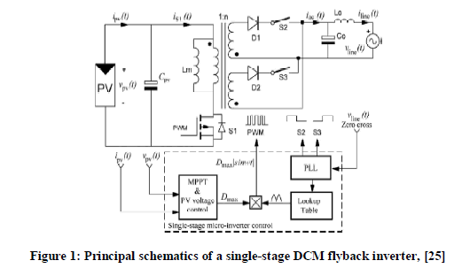
| This Section provides the power system model in MATLAB Simpower system tool box, Photo Voltaic (PV) model, simulation results, design calculation to find the fly back capacitor value, and the simulation results. The physical circuit of the power system model is given in Figure 1 and the corresponding simpower system model and its implementation is given and discussed in this section. The detailed description of the power system model, input parameters used, output voltage and output current values are given. |
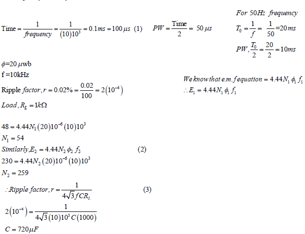
| Design Calculations: |
| The frequency of the system is 10 kHz |
 |
SIMULATION MODEL AND RESULTS |
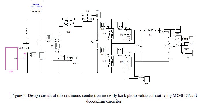
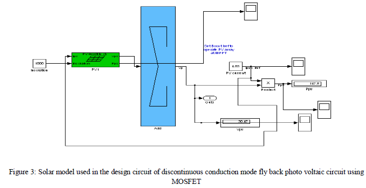
| The Photo voltaic module is shown in Figure 2 and the design of discontinuous conduction mode fly back photo voltaic micro inverters using decoupling capacitor circuit is given in Figure 3.Figure 2 consists of concentrated solar cells and produces the output voltage of 48.75 volt. The input parameters such as short-circuit current, open circuit voltage, current at Pmax and voltage at Pmax of the solar module is shown in the PV masked subsystem in Figure 4. The maximum power utilization of the PV module is calculated as given below and is shown in the PV model in sim power system toolbox Figure 2. |
 |
| Output voltage of the PV module = 48.75 volt, Output current of the PV module = 4.85 amps PV power utilization = Voltage ( PVCurrent)=48.75(4.85)=236.43 Watts. |
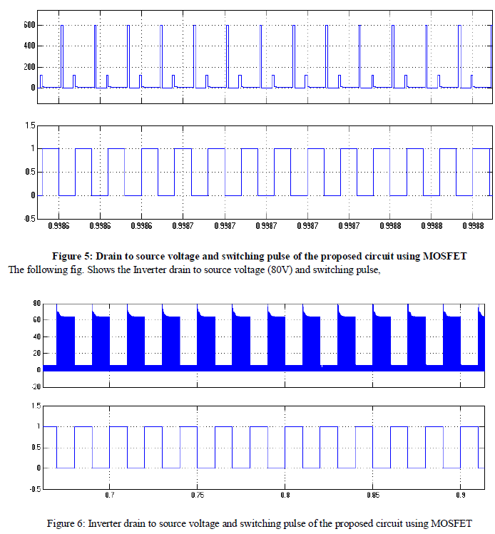
| The design circuit of the discontinuous conduction mode flyback photo voltaic microinverters using decoupling capacitor is given in Figure 3. The circuit consists of the input voltage of 48.75 volt generated using the concentrated solar cell and is shown in Figure 2. Input voltage of the PV module and drain to source voltage and switching pulse of the MOSFET are given in Figure 4 and Figure 5 respectively. This input voltage is given to the MOSFET circuit and its output of the MOSFET is given as input to the transformer primary. The primary and secondary voltage of the transformer is 50 and 12.5 volt respectively and the scope output which shows the transformer voltages is given in Figure 4. |
| It is noted that the proposed circuit given in Figure 2uses the fly back circuit using inverter and is modified to produce a output AC voltage in order to connect the PV power generation to the grid using MOSFET bridge circuit with RL load and its PV module circuit is given in Figure 3.The output response of the input voltage of the PV module, drain to source voltage and switching pulse, transformer primary voltage and secondary voltages, input current, transformer secondary side current, output voltage, output current, and output voltage reduced. |
 |
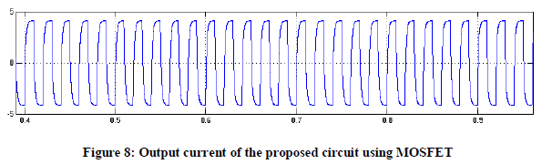
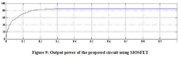
| The system responses for the proposed circuit using MOSFET (Figure 2) produces the following outputs such as: solar output voltage, drain to source voltage and switching pulse, inverter drain to source voltage and switching pulse, output voltage, output current, and output power are given in Figure 4 to 9 respectively. It is observed that the proposed circuit using MOSFET produces a AC outputs of 24 volt, 4.8 amps and 85 watts and the corresponding scope output is given in Figures 7 to 9 respectively. |
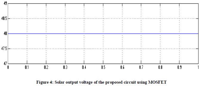
| The following fig. shows the output voltage of the solar PV panel (48V), |
 |
| The following fig. Shows the Drain to source voltage(600V) and switching pulse, |
 |
| The following fig. Shows the Output voltage, |
 |
| The following fig. Shows the Output current, |
 |
| The following fig. Shows the Output power, |
 |
DISCUSSION ON THE SIMULATION RESULTS |
| In this section the design circuit of discontinuous conduction mode flyback photo voltaic circuit using decoupling capacitor is proposed using MOSFET circuit with RL load (Figure 2). It is observed that the output voltage of the PV system without filter circuit has a ripple of 2% which is 2 volt output variation and the ripple has been reduced by adding the filter circuit in the output terminal of the PV system and the corresponding output voltage with 0.05 % ripple (which is 0.05 volt output variation. These output voltages are DC which cannot be connected to AC grid. The proposed circuit using MOSFET with RL load in Figure 2. |
CONCLUSION |
| This project has presented the procedures for the decoupling capacitor value for DCM fly back micro inverters is investigated, considering the PV power utilization and the THD of the inverter output current. Simulations and experimental results indicate that the decoupling capacitor value influences the THD more than the PV power utilization. Using this relationship, a novel decoupling capacitor selection method for single-stage and two-stage DCM fly back micro inverters is proposed. For single-stage inverters, the decoupling capacitor is placed across the PV output terminals, and should be sized according to the desired THD limit instead of PV power utilization. For two-stage inverters, the control method of the dc–dc converter determines the stage where the decoupling function takes place. Thus, the PV side decoupling capacitor should be dimensioned according to the PV power utilization ratio, and the inverter side decoupling capacitor should be selected according to the desired THD limitation. The basic circuit and modified circuit elements are designed using relevant equations. The simulation circuits are developed using elements of SIMULINK library. The Simulation is successfully done and open loop / closed loop simulation results are presented. The Simulation results coincide with the theoretical results. |
References |
|