International Journal of Advanced Research in Electrical, Electronics and Instrumentation Engineering
ISSN ONLINE(2278-8875) PRINT (2320-3765)
ISSN ONLINE(2278-8875) PRINT (2320-3765)
B. Suresh Kumar1, GantaJoga Rao2
|
| Related article at Pubmed, Scholar Google |
Visit for more related articles at International Journal of Advanced Research in Electrical, Electronics and Instrumentation Engineering
In the microgrid system, single-phase inverter is usually used for the distributed energyresource (DER). To reduce conversion losses, Removing the transformer and reducing power devices will bring down the cost and zise of the converter. The objective of this paper is to build simulation of seven levelmultistring inverter topology for DERs based DC to AC system. In this paper, a high step-up converter isused as front-end stage to improve the conversionefficiency of conventional boost converters and to stabilize theoutput DC voltage of various DERs such as PV and fuel cellmodules for use with the simplified multilevel inverter. Seven level inverter requires only six active switchesinstead of the eight required in the conventional cascaded H-bridgeinverter. In addition, two activeswitches are operated under line frequency. The simulatedseven level string inverter topology offers strong advantages such asimproved output waveforms, small filter size, and lowmagnetic interferenceand harmonic distortion. Simulation results show theeffectiveness of the proposed solution.
Keywords |
| DC/AC power conversion, multilevel inverter |
INTRODUCTION |
| In light of public concern about global warming and climatechange, much effort has been focused on development ofenvironmentally friendly distributed energy resources (DERs).For delivering premium electric power in terms of highefficiency, reliability, and power quality, integrating interfaceconverters of DERs such as photovoltaic, wind power, microturbines, and fuel cells into the microgrid system has become acritical issue in recent years [1]-[4]. In such systems, mostDERs usually supply a DC voltage that varies in a wide rangeaccording to various load conditions. Thus, a DC/AC powerprocessing interface is required and is compliable withresidential, industrial, and utility grid standards [4]-[7].Various converter topologies have been developed forDERs [7]-[16] that demonstrate effective power flow controlperformance whether in grid-connected or stand-aloneoperation. Among them, solutions that employ highfrequency transformers or make no use of transformers at all have beeninvestigated to reduce size, weight, and expense. For lowmediumpower applications, international standards allow theuse of grid-connected power converters without galvanicisolation, thus allowing so-called âÃâ¬Ãâ¢transformerlessâÃâ¬Ãâarchitectures [7], [12]. Furthermore, as the output voltage levelincreases, the output harmonic content of such invertersdecreases, allowing the use of smaller and less expensiveoutput filters. As a result, various multilevel topologies are usually characterized by a strong reduction in switchingvoltages across power switches, allowing the reduction ofswitching power losses and electromagnetic interference (EMI)[8], [11]. A single-phase multistring five-level inverterintegrated with an auxiliary circuit was recently proposed forDC/AC power conversion [12], [13]. This topology used in thepower stage offers an important improvement in terms oflower component count and reduced output harmonics.Unfortunately, high switching losses in the additional auxiliarycircuit caused the efficiency of the multistring five-levelinverter to be approximately 4% less than that of theconventional multistring three-level inverter [13]. In [14], anovel isolated single-phase inverter with generalized zero vectors (GZV) modulation scheme was first presented tosimplify the configuration. However, this circuit can still onlyoperate in a limited voltage range for practical applicationsand suffer degradation in the overall efficiency as the dutycycle of the DC-side switch of the front-end conventionalboost converter approaches unity [6], [14]. Furthermore, theuse of isolated transformer with multi-windings of the GZV based inverter results in the larger size, weight, and additionalexpense [14].To overcome the above-mentioned problem, the objectiveof this paper is to study a newlyconstructed transformerlessfive-level multistring inverter topology for DERs. In this paper,the foresaid GZV-based inverter is reduced to a multistringmultilevel inverter topology that requires only six activeswitches instead of the eight required in the conventionalcascaded H-bridge (CCHB) multilevel inverter [16]. Inaddition, among them, two active switches are operated underline frequency. In order to improve the conversion efficiencyof conventional boost converters, a high step-up converter [26]is also introduced as a front-end stage to stabilize the outputDC voltage of each DER modules for use with the simplifiedmultilevel inverter. The newly-constructed inverter topologyoffer strong advantages such as improved output waveforms,smaller filter size, and lower EMI and total harmonicsdistortion (THD). In this paper, the operating principle of thedeveloped system is described, and a Simulation is constructedfor verifying the effectiveness of the topology. |
 |
SYSTEM CONFIGURATION OF OPERATION PRINCIPLES |
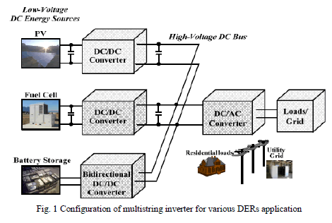
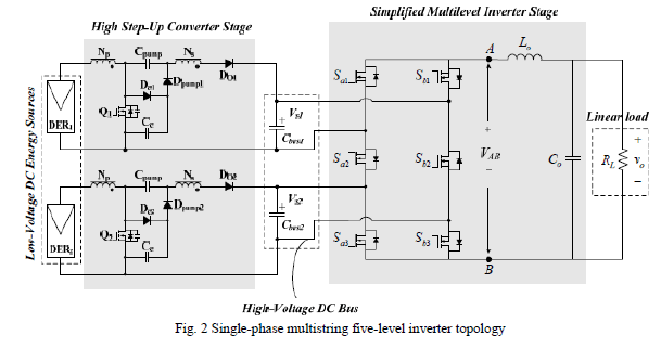
| A general overview of different types of photovoltaic (PV) modules or fuel cell inverters is given in [9]. Thispaper presents a multistring multilevel inverter for DERs application. The multistring inverter shown in Fig. 1 is a further development of the string inverter, whereby several strings are interfaced with their own DC/DC converter to a common inverter. This centralized system is beneficial because each string can be controlled individually. Thus, the operator may start his own PV/fuel cell power plant with a few modules. Further enlargements are easily achieved because a new string with a DC/DC converter can be plugged into the existing platform, enabling a flexible design with high efficiency [9]. The single-phase multistring multilevel inverter topology used in this study is shown in Fig. 2. This topology configuration consists of two high step-up DC/DC converters connected to their individual DC bus capacitor and a simplified multilevel inverter. Input sources, DER module 1, and DER module 2 are connected to the inverter followed a linear resistive load through the high step-up DC/DC converters. The studied simplified five-level inverter is used instead of a conventional phase disposition (PD) pulse width modulated (PWM) inverter because it offers strong advantages such as improved output waveforms, smaller filter size, and lower electromagnetic interference and THD. It should be noted that, by using the independent voltage regulation control of the individual high step-up converter, voltage balance control for the two bus capacitors Cbus1, Cbus2 can be achieved naturally. |
| A. High Step-Up Converter Stage: |
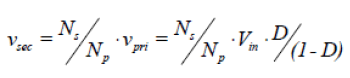
| In this study, high step-up converter topology is introduced to boost and stabilize the output DC voltage of various DERs such as PV and fuel cell modules for employment of the proposed simplified multilevel inverter. The architecture of a high step-up converter initially introduced from, depicted in Fig. 2, and is composed of different converter topologies: boost, flyback, and a charge pump circuit. The coupled inductor of the high step-up converter in Fig. 2 can be modelled as an ideal transformer, a magnetizing inductor, and a leakage inductor. According to the voltage seconds balance condition of the magnetizing inductor, the voltage of the primary winding can be derived as whereVin represents each the low-voltage DC energy inputsources, and voltage of the secondary winding isSimilar to that of the boost converter, the voltage of thecharge-pump capacitor Cpumpand clamp capacitor Cc can beexpressed as |
 |
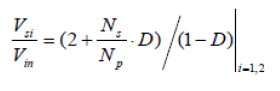
| Hence, the voltage conversion ratio of the high step-upconverter, named input voltage to bus voltage ratio, can bederived as [26] |
 (2) (2) |
| B. Simplified Multilevel Inverter Stage |
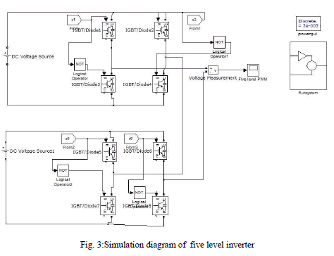
| To assist in solving problems caused by cumbersome powerstages and complex control circuits for conventional multilevelinverters, this work reports a new single-phase multistringtopology, presented as a new basic circuitry in Fig. 3.Referring to Fig. 2, it should be assumed that, in thisconfiguration the two capacitors in the capacitive voltagedivider are connected directly across the DC bus, and allswitching combinations are activated in an output cycle. Thedynamic voltage balance between the two capacitors isautomatically controlled by the preceding high step-upconverter stage. Then, we can assume Vs1=Vs2=Vs. |
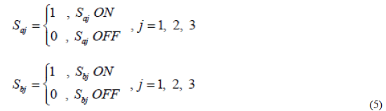
| This topology includes six power switches—two fewer thanthe CCHB inverter with eight power switches— whichdrastically reduces the power circuit complexity and simplifiesmodulator circuit design and implementation. The PD PWMcontrol scheme is introduced to generate switching signals andto produce five output-voltage levels: zero, VS, 2VS, -VS, and -2VS. This inverter topology uses two carrier signals and onereference to generate PWM signals for the switches. Themodulation strategy and its implemented logic scheme in Fig.4(a) and (b) are a widely used alternative for phase dispositionmodulation. With the exception of an offset value equivalentto the carrier signal amplitude, two comparators are used inthis scheme with identical carrier signals Vtri1 and Vtri2 toprovide high-frequency switching signals for switches Sa1, Sb1,Sa3 and Sb3. Another comparator is used for zero crossingdetection to provide linefrequency switching signals forswitches Sa2 and Sb2. |
| For convenient illustration, the switching function of theswitch in Fig. 3 is defined as follows:Table I. lists switching combinations that generate therequired five output levels. The corresponding operationmodes of the multilevel inverter stage are described clearly asfollows: |
 (4) (4) |
| (1) Maximum positive output, 2VS: Active switches Sa2, Sb1,and Sb3 are on; the voltage applied to the L-C output filter is2VS. |
| (2) Half-level positive output, +Vs: This output condition canbe induced by two different switching combinations. Oneswitching combination is such that active switches Sa2, Sb1, Sa3are on; the other is such that active switches Sa2, Sa1, Sb3 are on.During this operating stage, the voltage applied to the L-Coutput filter is +Vs. |
| (3) Zero output, 0: This output condition can be formed byeither of the two switching structures. Once the left or rightswitching leg is on, the load will be short-circuited, and thevoltage applied to the load terminals is zero. |
| (4) Half-level negative output, -Vs: This output condition canbe induced by either of the two different switchingcombinations. One switching combination is such that activeswitches Sa1, Sb2, Sb3 are on; the other is such that activeswitches Sa3, Sb1, Sb2 are on. |
| (5) Maximum negative output, -2Vs: During this stage, activeswitches Sa1, Sa3, and Sb2 are on, and the voltage applied to the L-C output filter is -2Vs.In the these operations, it can be observed that the openvoltage stress of the active power switches Sa1, Sa3, Sb1, Sb3 areequal to input voltage VS; moreover, the main active switchesSa2 and Sb2 are operated at the line frequency. Hence, theresulting switching losses of the new topology are reducednaturally, and the overall conversion efficiency is improved.To verify the feasibility of the single-phase five-levelinverter, a widely used software program PSIM is applied tosimulate the circuit according to the previously mentionedoperation principle. The control signal block is shown in Fig. 4;m(t) is the sinusoidal modulation signal. |
 |
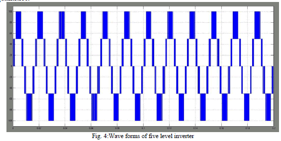
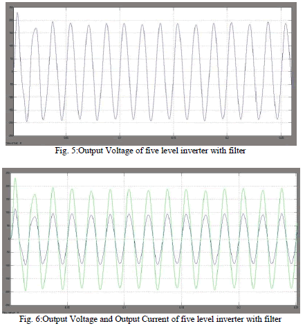
| Both Vtri1 and Vtri2 arethe two triangular carrier signals. The peak value and frequency of the sinusoidal modulation signal are given asmpeak=0.7 and fm=60Hz, respectively. The peak-to-peak value of the triangular modulation signal is equal to 1, and theswitching frequency ftri1 and ftri2 are both given as 1.8kHz.The two input voltage sources feeding from the high step-upconverter is controlled at 100V, i.e. Vs1=Vs2=100V. Thesimulated waveform of the phase voltage with five levels isshown in Fig. 5. The switch voltages of Sa1, Sa2, Sa3, Sb1, Sb2,and Sb3 are all shown in Fig. 6. It is evident that the voltagestresses of the switches Sa1, Sa3, Sb1, and Sb3 are all equal to100V, and only the other two switches Sa2, Sb2 must be 200Vvoltage stress. |
 |
| C. Comparison with CCHB inverter |
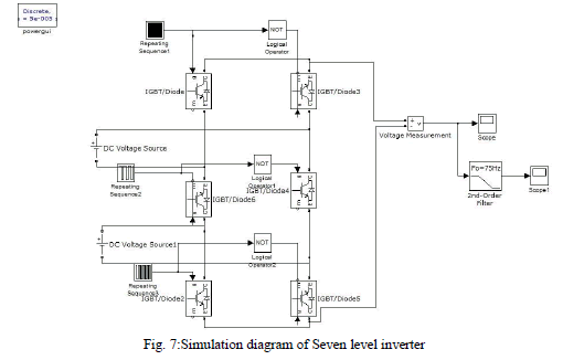
| The average switching power loss Ps in the switch causedby these transitions can be defined as where tc(on) and tc(off) are the turn-on and turn-off crossoverintervals, respectively; VDS is the voltage across the switch;and Io is the entire current which flows through the switch.Compared with the CCHB circuit topology as shown in Fig.7, the voltage stresses of the eight switches of the CCHBinverter are all equal to Vs.For simplification, both the proposed circuit and CCHBinverter are operated at the same turn-on and turn-offcrossover intervals and at the same load Io. Then, the averageswitching power loss Ps is proportional to VDS and fsas According to Eq. (8), the switching losses ofthe CCHB inverter from eight switches can be obtained as Similarly, the switching power loss of the proposed singlephasefivelevel inverter due to six switches can also beobtained as Because switches Sa2, Sb2 can only be activated twice in aline period (60Hz) and the switching frequency is larger thanthe line frequency (fs>>fm), the switching losses of theproposed circuit is approximated to 4Vsfs . Obviously, theswitching power loss is nearly half that of the CCHB inverter. Considering the harmonics in the inverter output voltageVAB, the amplitude of the fundamental and harmoniccomponents in the output voltage VAB are calculated by PSIMsoftware. The phase shift PWM technique is adopted for theCCHB Inverter. Both of the CCHB multilevel inverter and thestudied multilevel inverter are operated in the same condition,including the same switching frequency 18kHz, the samemodulation index ma ,the same input voltage VS=100V andoutput L-C filter, Lo=420uH, Co=4.7uF. |
SIMULATION RESULTS |
| To facilitate understanding of the operating principle and as verification, a Simulation system with a high step-up DC/DC converter stage and the simplified multilevel DC/AC stage are built with the corresponding parameters listed. The specifications of the two preceding high step-up DC/DC converters are (a) input voltage 30V; (b) controlled output voltage 100V; and (c) switching frequency 85kHz. The corresponding specifications of the simplified multilevel DC/AC inverter stage are (1) output power, Po=230W; (2) input voltage, Vs=100V; (3) output voltage, vo=110Vrms; (4) line frequency, fm=60Hz; (5) switching frequency, fs=40kHz; and (6) peak modulation index, mpeak=0.76. For better understanding, the guidelines and considerations of the DC-link capacitance and the use of an L-C output filter at the output are described as follows. |
| A. Sizing DC-link capacitor |
| For the discussed two-stage DC/AC conversion system, the DC-link capacitance is sized to keep voltage fluctuations within specified limits to prevent over-voltage on the DC bus. |
 |
| To calculate the relationship between capacitance and voltage limits, the net power flowing into the bus capacitor, i.e. DClink capacitor, is expressed as where PDER is the total output power of the DER modules, and Vo and Io are the peak AC-side quantities. |
 |
| Assuming a steady-state operating condition whereby the net average power flow is zero, the instantaneous power flow into the bus capacitance Cbusis PDER cos 2wt . Integrating this expression provides the energy, and equating the peak change in energy stored in the capacitor with where Vbus,max is the peak bus voltage, Vbus,min is the minimum value of bus voltage, and Cbus=Cbus1×Cbus2/(Cbus1+Cbus2). The voltage deviation is given by For the discussed twostage conversion system in this study, a design limit of maximum ΔVbus=10V is chosen to keep the bus voltage well within the voltage rating of the semiconductors, which now is typically 200V, and to minimize the third-order harmonic occurring on the output voltage. |
 |
| For the above-mentioned considerations, the capacitance Cbus1 and Cbus1 are now chosen as 2000μF, respectively. It should be noted that, for simplification, the bus capacitance for this case is only selected based on voltage deviation specifications. |
 |
| B. Choice of output L-C filter |
| The output L-C filter is tuned to below the switching frequency as follows: where fsis the switching frequency, and Lo and Co are inductance and capacitance of the output L-C filter, respectively. The Simulation results of the simplified single-phase inverter stage operated at the rated output power are shown in Figs. 8-10. |
 |
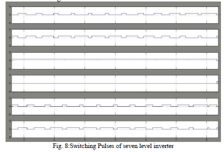
| Figs. 8-9 show the PWM signals and voltage stresses of the six power switches for the five-level inverter, respectively. It is evident that the voltage stresses of the switches Sa1, Sa3, Sb1, and Sb3 are all equal to 100V, and only the other two switches Sa2, Sb2 must be 200V voltage stress. |
 |
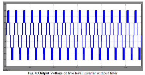
| Fig.9 shows steadystate waveforms of output voltage vo, output current io, and the voltage applied to L-C output filter terminal VAB, respectively, for the inverter with a resistive load of 51Ω. |
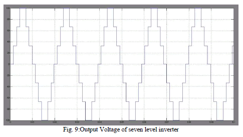 |
| As can be seen in Fig. 8, the waveform shows the desired five voltage levels: 200V, 100V, 0V, -100V, and -200V. The measured RMS value of vois approximately 110V, while the measured RMS value of iois approximately 2.12A. The conversion efficiency of the implemented inverter and THD of the output voltage measured in this case are approximately 96% and 3%, respectively. |
CONCLUSION |
| This work reports a newly-constructed single-phase multistring multilevel inverter topology that produces a significant reduction in the number of power devices required to implement multilevel output for DERs. The studied inverter topology offer strong advantages such as improved output waveforms, smaller filter size, and lower EMI and THD. Simulation results show the effectiveness of the proposed solution.This paper presents a new Novel Asymmetrical Multistring multilevel converter. Here we proposed single phase and three phase multistring multilevel inverters, the proposed converter produces more voltage levels with less number of switches compared to H- bridge configuration. This will reduce the switching losses and number of gate drivers and protection circuits which in turn reduces the cost and complexity of the circuit. Finally a three phase model of the proposed circuit is shown and simulation results are presented. |
References |
|