International Journal of Advanced Research in Electrical, Electronics and Instrumentation Engineering
ISSN ONLINE(2278-8875) PRINT (2320-3765)
ISSN ONLINE(2278-8875) PRINT (2320-3765)
| Blessen Antony Francis1, Bos Mathew Jos2, Babu Thomas3 Department of Electrical and Electronics Engineering, Mar Athanasius College of Engineering, Kothamangalam, Kerala, India |
| Related article at Pubmed, Scholar Google |
Visit for more related articles at International Journal of Advanced Research in Electrical, Electronics and Instrumentation Engineering
The conventional full-wave diode bridge rectifier with an output capacitor filter produces current spikes in the supply, thus lowering the power factor and distorting the waveform. An ideal rectifier presents an effective resistive load (Emulated resistance) to the AC power line; hence, if the supplied AC voltage is sinusoidal, then the current drawn by the rectifier is also sinusoidal and is in phase with the voltage. Converters that approximate the properties of the ideal rectifier are sometimes called power factor corrected, because their input power factor is nearly unity. The boost converter, as well as a variety of other converters, can be controlled such that a near ideal rectifier system is obtained. This is accomplished by control of a high-frequency switching converter, such that the ac line current waveform follows the applied ac line voltage. The boost converter is operated in Continuous Conduction Mode (CCM), and controlled by Average Current Mode Control (ACMC). The system contains multi-loop control strategy and a feed-forward loop in order to get power factor near unity with constant output power. There are a variety of Power Factor Correction (PFC) chips available in the market, one being the UC3854, can be operated in Average Current Mode Control. The simulation of a 250W, AC – DC rectified system with Unity Power Factor at the input using UC3854 was done in PSIM Power Electronics simulation software and results were obtained.
Keywords |
| PFC-Power Factor Correction, CCM-Continuous Conduction Mode, ACMC-Average Current Mode control, CMC- Current Mode Control, PWM – Pulse Width Modulation, PI – Proportional plus Integral |
INTRODUCTION |
| AC to DC conversion basically requires a diode bridge and a filter capacitor. An increase in the power requirement and the betterment of DC output, demands large value of capacitors. This increases the non-sinusoidal current from the supply. The RMS value of current increase and there is a chance of tripping of the supply. Moreover, this non-sinusoidal current is an indication of harmonic content assuming sinusoidal supply voltage, and the power factor decreases [2, 3]. As the power factor decrease, the drawing of useful power decrease. Harmonics increase conduction losses. Hence, it is important to improve power factor and owing to this importance, standards were designed for regulating line current harmonics. There are passive and active power factor correction methods [1]. |
| The method of power factor correction used here is the active type and it is current mode control. The current mode control (CMC) strategy used is the averaged current mode control, which is an extension of the peak CMC. Peak CMC is discussed in detail [4], with modelling of the same, and a basic control system block diagram provided, which form the basic idea. Peak current control is the control of the peak current through the switching element. Peak current mode control requires an additional ramp for stability, there is no need for current loop compensation. |
| When the ripple in the inductor current is less, peak current mode becomes similar to average current mode control (ACMC). Here, the average current through the inductor is sensed. Any current can be controlled using this method. Average CMC require two loops viz. a fast current loop(Large bandwidth), and comparatively low band width voltage loop. Paper [5] is a continuation of [4], explaining additional blocks in the control system modelling of average CMC |
| when compared to the peak CMC. The control system modelling of ACMC in [6] is done by modelling the PWM switch, and a buck converter is explained. |
| In paper [7], the issues of peak CMC, the current loop design for an average CMC in a buck converter, a boost preregulator and a flyback regulator, and different practical aspects of current sensing are discussed. The current loop transfer function and control loop design for this work is obtained from this reference [7]. Paper [8] discusses about the voltage loop modelling and transfer function of the boost PFC circuit, and provides different transfer functions for resistive load and a constant power load to the boost PFC circuit. When we are connecting a constant power load, i.e., a DC-DC converter, the constant power load represents a negative resistive load. Hence, a constant power load should not be connected to the boost PFC unless it is tightly regulated (close-loop controlled). |
| The basic pre-regulator operation, presence double line frequency component at the output, different power circuit topologies for PFC, control loop design criteria, the need of a input voltage feed-forward loop for PFC, average CMC design, small signal model of voltage loop can be found in [9], which is an extension of [8]. The paper also gives some valuable suggestions on load over current limiting and practical aspects of control circuit DC offsets. [10] Discusses about peak and average CMC control of boost PFC circuit. An in-site to current loop compensation procedure is provided. [11] Provides small signal model of the required average CMC boost PFC circuit. The block diagram provided can be read as an extension from [4] and [5]. The modelling of the multiplier is done [11] and is incorporated into the work of [5]. The current and voltage loop transfer functions, the design guidelines for the compensation of the same for the thesis work are obtained from this reference. |
| [13]Discusses the sources of harmonic distortion in boost PFC circuit, an initial design example of the boost converter, setting up of the multiplier and divider, voltage loop and feed-forward loop design guidelines. Sources of harmonic distortion in the PFC circuit, and the ways to reduce the same can be obtained from [12]. Important aspects on practical design issues for PFC circuits, especially on-line filtering, loop compensation, input voltage feed-forward, protection circuits and the need for switching signal synchronisation (meant for constant power load) are addressed in [14]. |
| [15]Introduces the UC3854 power factor correction chip for average CMC boost PFC circuit, which forms the heart of the work.[16] Provides guidelines on using the chip, and [17] provides steps for protection and optimisation of the boost PFC circuit. [18] Provides in-site for physical implementation of compensator design based on op-amps. |
| The design and simulation of a 250 W, AC-DC converter is carried out, with 400VDC obtained at the output. The simulation is done using a resistive load, and then with a closed loop 385 V/ 50V, 5A (250 W) DC-DC buck converter. The controller for buck converter can be used for forward converter (A buck converter derivative, with turns ratio 1:1) also, in case isolation is required. The simulation is done for similar load conditions for resistive and constant load converter loads. The control system design was done with the aid of MATLAB Version 7.10 (R2010b). Simulation of AC-DC converter was done in PSIM 64-bit Professional Version 9.0.3.464, using the UC3854 subsystem block. |
OPERATION PRINCIPLE OF ACMC BOOST PFC CONVERTER |
| A conceptual circuit diagram is obtained from [10] is reproduced below (a), along with the block diagram of the system (b) from [11] |
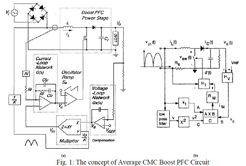 |
| The system mainly consists of: |
| Uncontrolled full wave diode bridge rectifier and a boost power stage |
| A high bandwidth current feedback loop with compensator. |
| A very low bandwidth Voltage feedback loop with compensator. |
| Voltage feed-forward loop through a low pass filter (LPF). |
| An input rectified-sinusoidal current reference signal. |
| An analog signal multiplier and divider. |
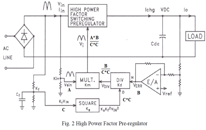
| The Fig.2 from [9] provides more insight of the working. |
 |
| A part of output voltage is compared with the reference to get an error signal (B), this is fed to the multiplier. A signal (A), rectified sinusoidal signal is another input to the multiplier. These two signals can produce a rectified sinusoidal control signal to the reference of current loop compensator, thus to obtain a unity PF i.e., sinusoidal input current at input of the AC-DC converter. |
| In this context it can be noticed that when voltage and current are in phase power drawn is increased, and one of our requirement being constant power is violated. The load can be either a resistor or a DC-DC converter. So in-order to make power drawn independent of change in input RMS voltage a voltage feed-forward is utilised. The feed-forward voltage is squared at the denominator and fed to the multiplier. A low pass filter in the way of feed-forward signal is to step down the input voltage and to attenuate third harmonic ripple current in AC line from entering to the system, as explained in [12]. |
| The voltage loop is so slow that for the half sinusoid of input AC line, the divider output is a constant referring to Fig.2. The output of the multiplier is then a rectified sinusoidal signal as reference to the current loop. This is like a rectified-sinusoidal reference input to the controller a DC-DC converter, for which its output control signal should be such that the output of the DC-DC converter should be a rectified-sinusoidal voltage. This is possible if the current loop is a very fast acting one, having high bandwidth. In this case the output signal is the sensed average inductor current. This makes current and voltage in phase, i.e. high PF. This fact is visible from Fig.1 (a). The Rs in Fig.1 (b) is the sense resistor for sensing the average inductor current or the input current. |
DESIGN SPECIFICATIONS |
| The design specification for the converter is the first step for design. |
| Input voltage = 230Vrms |
| Line frequency = 50Hz |
| Output voltage, Vo = 385VDC |
| Maximum output power, Pout = 250W |
| Switching frequency, fs = 100kHz |
POWER STAGE DESIGN |
A. Boost Inductor |
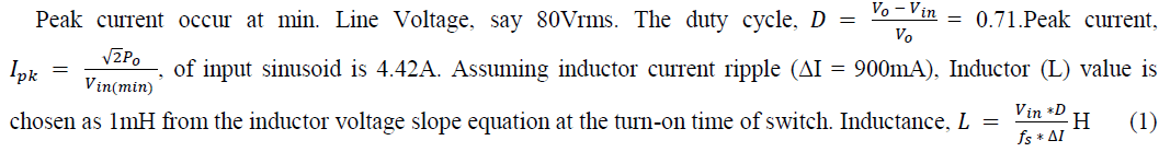 |
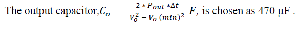
B. Output Capacitor |
| The output capacitor serves a purpose of a filter, power source for a small period of time etc., the design criteria includes: |
| Hold - up time, ΔT = 64mS |
| Decrease output voltage ripple |
| Decrease second harmonic ripple current |
 |
CONTROL BLOCK DIAGRAM OF ACMC BOOST PFC CONVERTER |
| The block diagram for the system is shown in Fig.3. The average CMC is an extension of peak CMC. The block diagram and a very good explanation on peak CMC can be obtained from [4]. When the peak current ripple is very small, peak CMC becomes equivalent to average CMC. Meanwhile, Average CMC includes a sensing resistor, current loop compensator and does not require slope compensation when compared to peak CMC. The control block diagram for average CMC can be obtained from [5]. The boost PFC circuit is an application of average CMC boost converter, which includes a multiplier and divider as extra components. A mathematical mode for the multiplier-divider block can be obtained from [11]. On combining [4, 5, 11], the following control block diagram is obtained. |
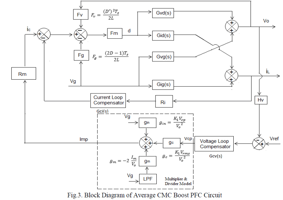 |
| The Riis the sense resistor, Imp is the current controlling signal through Rm. D, Duty cycle, Ts, switching period, Vg is the input voltage, Vo, the output voltage, Gvd(s), the control to output voltage transfer function, Gid(s) control to current transfer function, Gvg(s), the voltage input to output transfer function, Gig(s), the current input to output transfer function. Here, it is the output voltage and the inductor current, IL that is to be controlled. The block diagram is a merger of mathematical modelling and physical appearance. This control block diagram is a must when dealing with compensation of loops. |
INNER CURRENT CONTROL LOOP |
A. Controller Design |
 |
| triangular carrier for PWM generation. The PWM switch model when applied to boost converter [10], the small signal equivalent circuit is as shown in Fig.4 (a). |
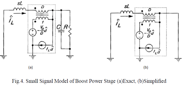 |
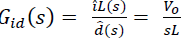
| Since output capacitor large, capacitor can be thought of a constant voltage source. At high frequencies, capacitive reactance is very low and can be modelled as short circuit Fig.4 (b). By circuit analysis, referring voltage source to 1° side of the transformer, output inductor current to control transfer function, |
 |
1) Current Loop Compensation Strategy |
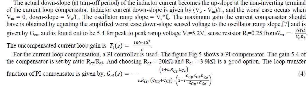
| The loop cross-over frequency is to be made16 kHz, and the Phase Margin is to be increased above 45° for stable system. For this, a zero is added at 12 kHz and a pole is added at 128 kHz. |
2) Current Loop Compensation Design |
 |
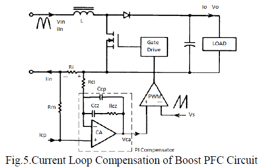 |
| To increase the phase margin of the current loop, the compensator zero is placed at the cross-over frequency, fci = 15.9 kHz. Using numerator of Eqn.6.7, Ccz is chosen as 680 pF. A pole is added above 50 kHz to attenuate noise. Using denominator of Gci(s), Ccp is chosen as 68pF. The compensated system exhibits a cross-over frequency of 16.67 kHz and a phase margin of 47.53° is obtained. |
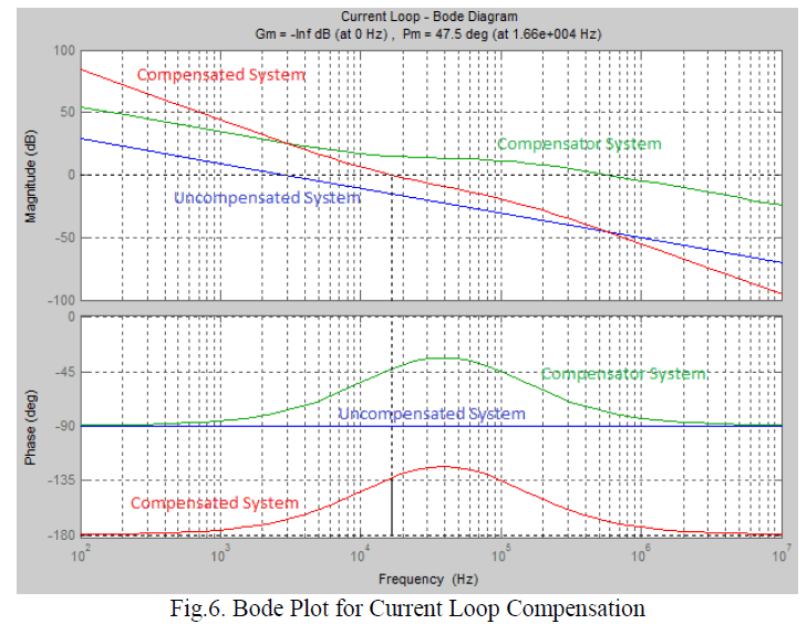
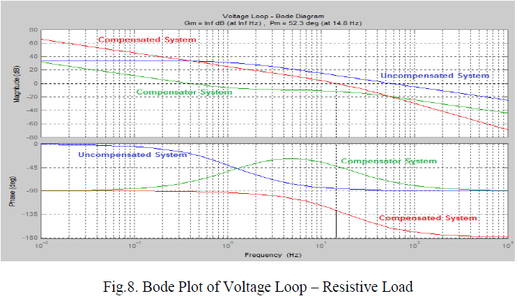
B. Frequency Response Analysis |
| The bode plots of uncompensated, compensator and compensated system are merged together for a better understanding. |
 |
OUTER VOLTAGE CONTROL LOOP |
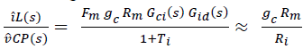
| From Fig.3, using Mason's gain formula, the control voltage to inductor current transfer function with closed current loop is given by [11], |
 |
 |
1) Compensation strategy |
| The compensator zero is placed at 2/RC and the compensator pole is added at 19 Hz. The cross-over frequency obtained should be a maximum 19 Hz. |
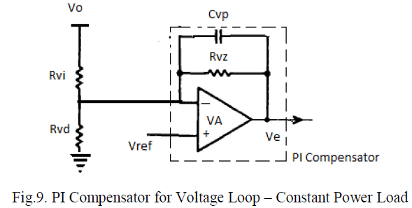
| Since the system is of single pole, a PI controller is used for compensation. |
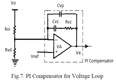 |
| The loop transfer function of PI compensator is given by, |
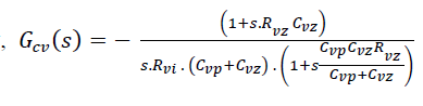 |
| Rvi is chosen 511kΩ. Cvp is chosen such that to attenuate double frequency ripples. It is chosen such that to get a gain of 0.0326 at double frequency, and is found out to be 47nF.As a strategy a zero is placed at 2/RC, ie, 1.19Hz. Cvz is chosen as 754nF. A pole is added at at 19.1Hz.Rvz is chosen as 177kΩ.Rvdis chosen as 10kΩ to get a voltage of 7.5V for a 385Voutput. |
2) Frequency Response Analysis |
 |
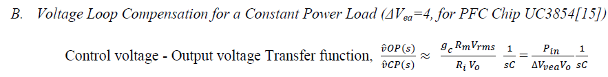 |
1) Compensation strategy |
| Here, the compensator pole is added at 19 Hz. The cross-over frequency obtained should be a maximum of 19 Hz. |
| A single pole is added for compensation. |
 |
| The loop transfer function of compensator is given by, |
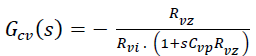 |
| All the components chosen are respectively the same as that of the resistive load case. |
| 2) Frequency Response Analysis |
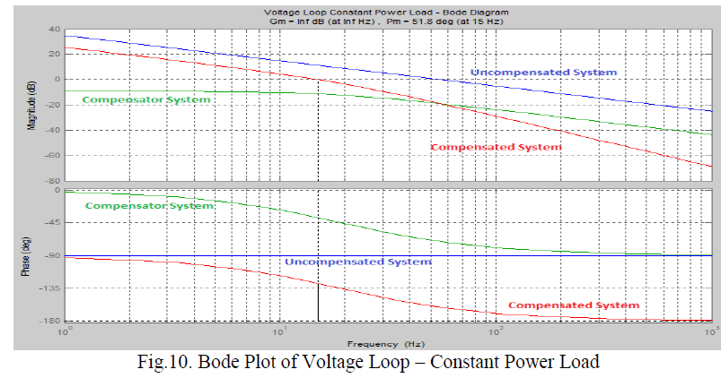 |
FEED-FORWARD LOOP DESIGN |
 |
| The feed-forward loop is designed to get the instantaneous input voltage, and is used to provide constant power at variable input voltage. So stepping down of the voltage is done by resistances. The output of feed-forward network is designed such that to get a voltage equal to 4.5 V at 270V rms, and 1.4V at 80V rms, for this the resistances Rff1, Rff2 and Rff3 are chosen as 910 kΩ, 91 kΩ and 20 kΩ respectively. The feed-forward loop can introduce 3rd harmonics of input current into the system. To attenuate this, two poles are added at a cut-off frequency 15 Hz. This is designed such that to get a gain of 0.15 at 100 Hz. Cut-off frequency is used to calculate values for filter capacitance, since here, the impedance of capacitance is equal to impedance of resistance. Cff1 and Rff2 form a pole at 18 Hz, giving Cff1 = 0.1 μF. Cff2 and Rff3 form a pole at 18 Hz, giving Cff2 = 0.47 μF. |
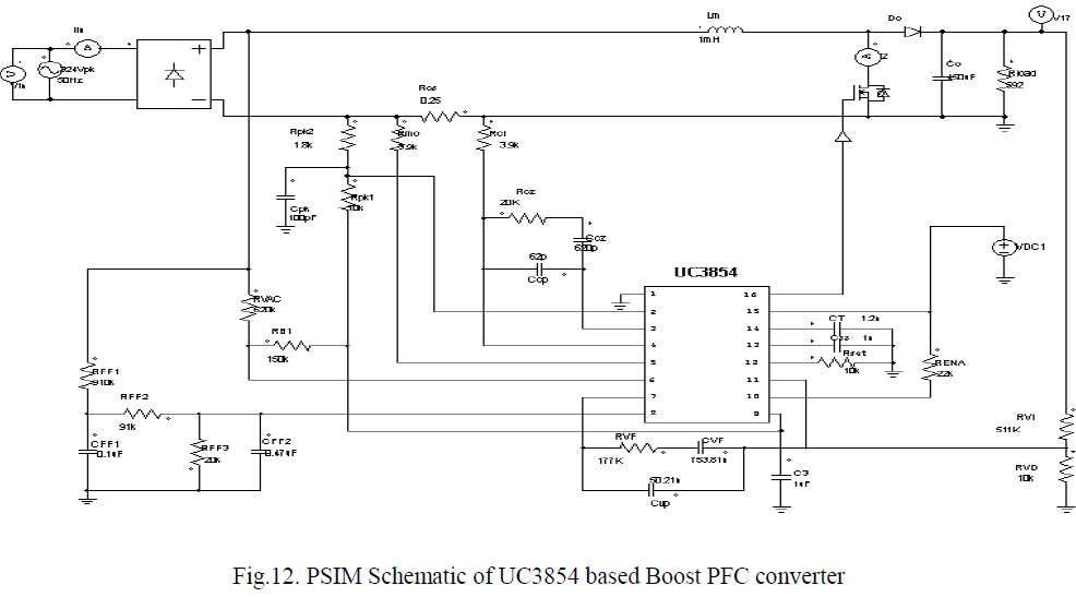
UC3854 PF REGULATOR |
| The components for the ACMC Boost PFC system can be discretised, owing to increase in number of components, cost etc. The UC3854 contains all the components for the purpose [15, 16, and 17]. The design for the multiplier and peak current limiting is obtained from [16]. |
SIMULATION AND EXPERIMENTAL RESULTS – RESISTIVE LOAD |
 |
 |
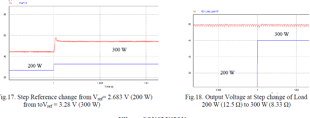
SIMULATION AND EXPERIMENTAL RESULTS – CONSTANT POWER LOAD |
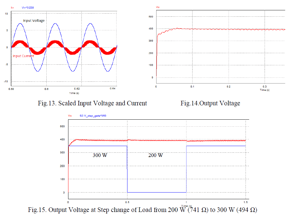
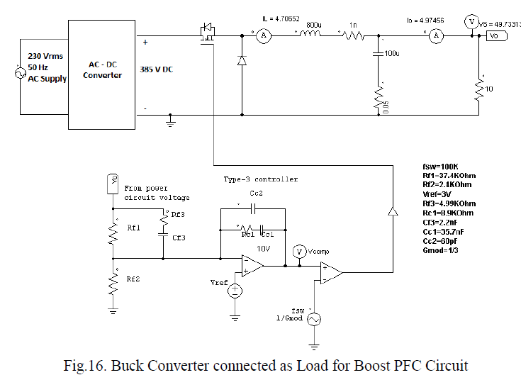 |
| A 385 V/50 V, 250 W, DC-DC closed loop buck converter was designed and simulated. Step reference and step voltage tests where done for similar conditions as that with the resistor load. |
 |
CONCLUSION |
| A 250 W, single phase PFC circuit based on ACMC boost converter was designed and simulated, with resistive load and constant power load, using UC3854 PFC Chip. For a resistive load, 385V DC is obtained as output from 230Vrms AC supply voltage and contains 120 Hz ripple. For a constant power load as buck converter, 50VDC is obtained at the output with very less ripples, and can be loaded up to 5 A. It is observed that, as the loading of PFC circuit increase; the input power factor is increased. Releasing the load degrades the power factor. This is observed in both resistive and constant-power loads. |
ACKNOWLEDGMENT |
| The authors wish to thank Dr. Mathews K. (Electronics and Communication Engineering Dept., Mar Athanasius College of Engineering, Kothamangalam) and Prof. George John P. (Electrical and Electronics Dept., Mar Athanasius College of Engineering, Kothamangalam)for his valuable opinions. Heartfelt thanks are extended to Mr.Nithin George (P.G. Scholar, M. A. C. E) for his valuable points. Special thanks to Mr.Vinjohn Chirackal (P.G. Scholar, Kyungpook National University, Republic of Korea). |
References |
|