International Journal of Advanced Research in Electrical, Electronics and Instrumentation Engineering
ISSN ONLINE(2278-8875) PRINT (2320-3765)
ISSN ONLINE(2278-8875) PRINT (2320-3765)
Siyana Ismail 1, Manjusha V.A2
|
| Related article at Pubmed, Scholar Google |
Visit for more related articles at International Journal of Advanced Research in Electrical, Electronics and Instrumentation Engineering
A bridgeless PFC rectifier allows the current to flow through a minimum number of switching devices compared to the conventional PFC rectifier. Accordingly, the converter conduction losses can be significantly reduced and higher efficiency can be obtained, as well as cost savings. In bridgeless cuk converter, only two semiconductor devices are working during one switching cycle and hence the conduction losses are minimised. CUK PFC rectifier is designed to operate in Discontinous Conduction Mode (DCM) to achieve almost a unity power factor and low total harmonic distortion of the input current. The simulation of both the closed loop based on average current mode control and open loop bridgeless cuk converter is carried out using MATLAB simulink. The closed loop model of the bridgeless cuk converter gives a higher power factor of 0.99 and better voltage regulation.
Keywords |
| Bridgeless rectifier, Cuk converter, low conduction losses, power factor correction (PFC) |
INTRODUCTION |
| Most electronic equipment is supplied by 50 Hz utility power, and more than 50% of this power is processed through some kind of power converter. Usually power converters use a diode rectifier followed by a bulk capacitor to convert AC voltage to DC voltage.Single phase diode rectifiers are widely used for industrial applications Since these power converters absorb energy from the AC line only when the line voltage is higher than the DC bus voltage, the input line current contains rich harmonics, which pollute the power system and interfere with other electric equipment. These converters usually have a low power factor of 0.65[1]. This introduces several problems including reduction in the available power and increased losses. This process involves both nonlinear and storage elements, and results in the generation of harmonics in the line current. Because the conventional simple diode rectifier followed by a bulk capacitor cannot meet the requirements, which have stimulated the research of power factor correction techniques. The concept of power factor originated from the need to quantify how efficiently a power converter utilizes the current that it draws from an AC power system. Power factor correction is the method of improving the power factor of a system by using suitable devices. The objective of power factor correction circuits is to make the input to a power supply behave like purely resistive or a resistor When a converter has less than unity power factor, it means that the converter absorbs apparent power higher than the real power it consumes. This implies that the power source should be rated with higher VA ratings than the load needs. In addition, the current harmonics produced by converter deteriorate the power source quality, which eventually affects the other equipment. |
| The two main methods to eliminate or atleast reduce the input line current harmonics are passive power factor correction and active power factor correction [2]. Because of low power factor offered by passive power factor correction, active methods are usually preferred. In active power factor correction, switching converters are used to shape the input current drawn by the ac/dc converter into a sinusoidal waveform that is in phase with the input voltage waveform. Buck, Boost and Buck-Boost converters are used. A bridge rectifier followed by a PFC has been the most commonly used PFC rectifier. But this bridge rectifier lowers the efficiency of the converter. This bridge rectifies the line voltage to feed the PFC stage with a rectified sinusoidal input voltage. It is well known that as a result of this structure, the input current must flow through two diodes before being processed by the PFC stage. An input bridge consumes about 2% of the input power at low line of a wide mains application. The need for higher efficiencies and low conduction losses from the PFC stage has led to bridgeless PFC converters. Several bridgeless PFC rectifiers have been introduced using buck boost [6] and SEPIC converter. Similar to the boost converter, the SEPIC converter has the disadvantage of discontinuous output current resulting in a relatively high output ripple. Bridgeless circuits with boost converter [5] and buck converters[4] were presented. In boost converter the dc output voltage is higher than the peak input voltage and it cannot be used for low power application such as for telecommunication [3]. By using the buck converter the input current does not track the input voltage at zero crossings of input voltage [4]. Also, buck PFC converter results in an increased total harmonic distortion (THD) and a reduced power factor. In my work bridgeless cuk rectifier is studied and simulated. The closed loop control of output voltage is done using average current mode control. |
BRIDGELESS CUK CONVERTER |
| The bridgeless cuk PFC rectifier shown in figure 1 is formed by connecting two dc-dc cuk converters in parallel. Each converter can operate for each half line period. The number of semiconductors in the current flowing path is reduced to one or two. Hence the circuit efficiency is improved compared to the conventional cuk rectifier. |
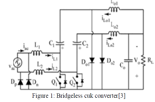 |
| The figure 1 shows the circuit diagram for bridgeless cuk converter. The Figure 2(a) shows the operation of bridgeless cuk rectifier during positive half cycle and Figure 2(b) shows the operation of bridgeless cuk rectifier during negative half cycle. |
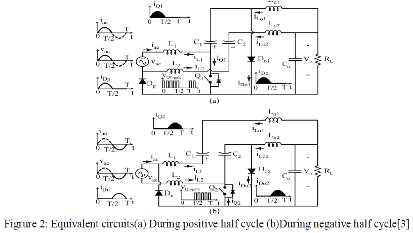 |
| Here during the positive half cycle switch Q1 is turned on. The current flowing path during this half cycle of supply voltage is through L1, Q1, C1 and D01. Dp is active during this cycle and it connects AC source to the output. During the negative half cycle switch Q2 is turned on. The current flowing path during the negative half cycle of supply voltage is through L2, Q2, C2 and D02. Dn is active during this cycle and it connects AC source to output. Here Dp or Dn connects the output voltage bus to input and thus common mode EMI noise emission can be eliminated. Control signals for the switch Q1 and Q2 can be controlled by the same control signals and hence the control circuitry is simple. |
2.1 Principle of operation |
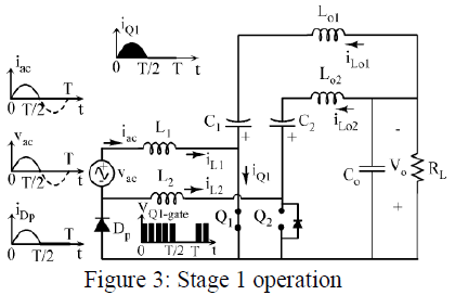
| The circuit operation during the positive and negative cycle of input voltage is same. Due to this symmetry of the circuit, it is sufficient to analyze the circuit operation during any one half cycle ie, positive half cycle. The circuit is analysed based on certain assumptions:- Input voltage is sinusoidal, components are ideal, all capacitors are large enough to reduce switching voltage ripple. The converter is operated in the Discontinuous Conduction Mode (DCM). The advantages offered by DCM operation include natural near-unity power factor, the power switches are turned ON at zero current, and the output diodes (D01 and D02) are turned OFF at zero current. Thus, the losses due to the turn- ON switching and the reverse recovery of the output diodes are considerably reduced. The circuit operation is divided into three distinct operating stages during one switching period. |
| Stage 1: In this stage Q1 is turned on. The current VC1 will flow through the switch and hence Dp is forward biased. The diode D01 is reverse biased by reverse voltage (Vac + V0). D02 is reverse biased by output voltage V0. The current through inductors iL1 and iL01 increases linearly with input voltage. Current through inductor iL02 is zero due to constant voltage across C2. The Stage 1 operation is shown in figure 3. |
 |
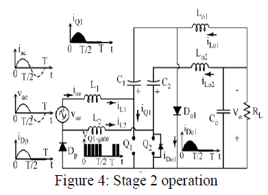
| Stage 2: In this stage switch Q1 is turned off. Diode D01 is turned on to provide path for inductor currents iL1 and iL01 . Dp is forward biased by the current iL1 . This stage ends when the current through diode D01 is zero. The Stage 2 operation is shown in figure 4. |
 |
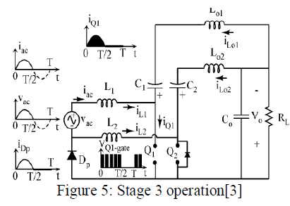
| Stage 3: During this interval both the switch and diode are revere biased. The inductors act as a current source and hence voltage across the inductors is zero. The current iL1 charges the capacitor. This stage ends when Q1 is turned on. The Stage 3 operation is shown in figure 5. |
 |
2.2 Design of the converter |
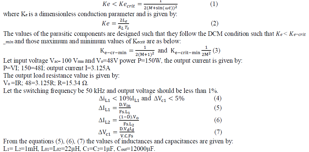
| The design of the converter is made as below with certain mathematical assumptions. The DCM operation is obtained with the following condition: |
 |
AVERAGE CURRENT MODE CONTROL |
| Average current mode control is used to control the shape of the input current and to regulate the output voltage [9]. The two major goals of controllers in PFC system: improved power factor and voltage regulation. The parameters used in the controllers to generate gate pulses of the switches are: input voltage, input current and output voltage. The inner loop is responsible for controlling the shape of the inductor current and the outer loop controls the output voltage and keeps it constant at the pre-defined reference value. In outer loop, the output voltage level is scaled and compared with the given reference. The error obtained from this comparison makes the input of the PI controller. The PI controller is designed to ensure the specifying desired nominal operating point for PFC converter, then regulating it, so that it stays very closer to the nominal operating point in the case of sudden disturbances, set point variations, noise, modelling errors and components variations. Output of this particular controller is the scaling factor and is used to obtain the current reference. |
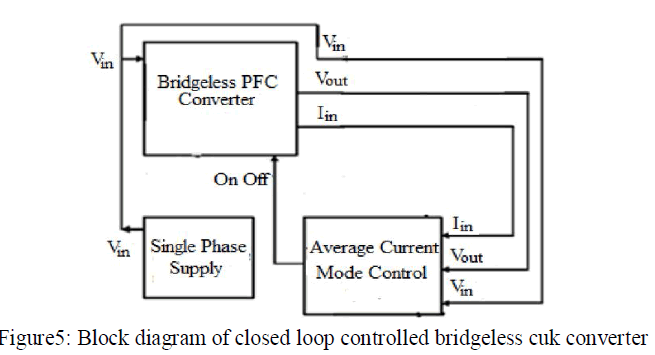 |
| In inner loop, the inductor current is compared with the reference current. The error of this comparison is processed by the different current controllers to be used to generate the gate signals of the switches. The block diagram of closed loop controlled bridgeless cuk converter is shown in Figure 5. Average current tracks the reference current with high degree of accuracy. This is especially important in high power factor converters. The average current mode control can be used to sense and control the current in any circuit branch. Fixed switching frequency and fast speed of response are other advantages of average current mode controller [8]. |
SIMULATION AND RESULTS |
| The circuit is simulated using MATLAB in Open loop mode and closed loop mode. Average current mode controller is used to stabilize the voltage. The simulink model and the simulation results of both the open loop and closed loop are shown below. Open loop bridgeless cuk converter is modeled, so the inrush current during start- up is not controlled and the output voltage is not stabilized. The inrush current and the output voltage can be controlled by using PWM of switches using closed loop control. |
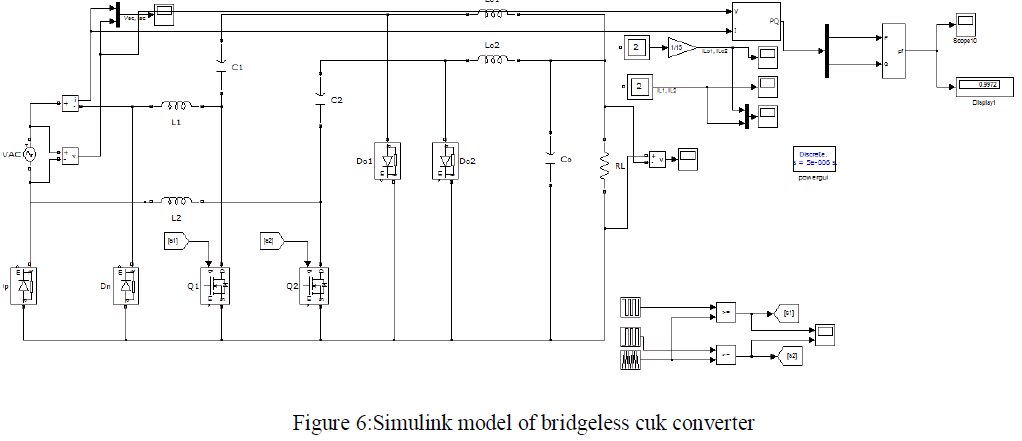 |
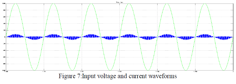
| The Figure 6 shows the simulink model of bridgeless cuk converter. The converter is modeled for 150W. The value of components used in this circuit is designed for 100V input voltage and 48V output voltage. The power factor obtained for open loop model is 0.9972. The input voltage and current waveforms are inphase and is shown in Figure 7.The output voltage waveform is not stabilized at 48V with the variation in input voltage |
 |
| The output voltage waveform for bridgeless cuk converter is shown in Figure8. |
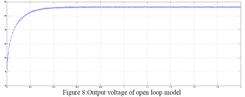 |
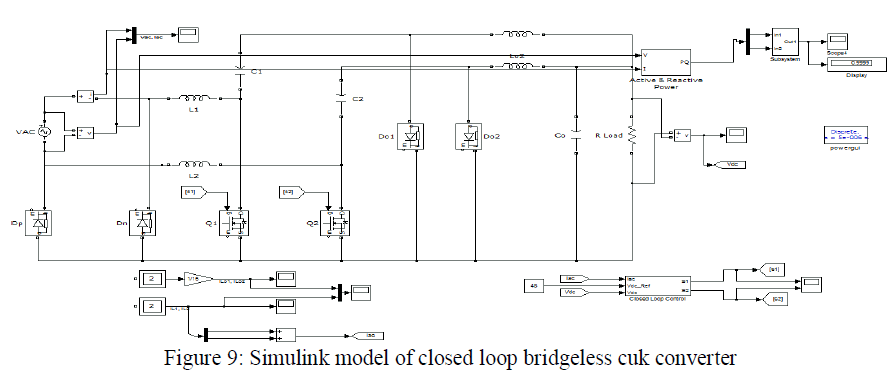
| Figure.7 shows the input voltage and input current waveforms. It is found that the phase difference between input voltage and input current is equal to zero. Here the power factor obtained is nearer to unity power factor and it is approximately 0.997. Figure 8 shows the output voltage waveform. An output voltage of approximately 48V is obtained. The output voltage will vary, if the input voltage is varied from 100V. Hence a closed loop model is developed for the bridgeless cuk converter. Simulink model of closed loop bridgeless PFC cuk converter is developed for input voltage 100V at 50Hz and output DC voltage of 48V and power rating of 150W. The output voltage is regulated by using the voltage controller loop and the shape of the input current is controlled by using the current controller loop. The PI controllers are used as the voltage controller and current controller. The simulink model of the closed loop bridgeless PFC cuk converter is shown in Figure 9. |
 |
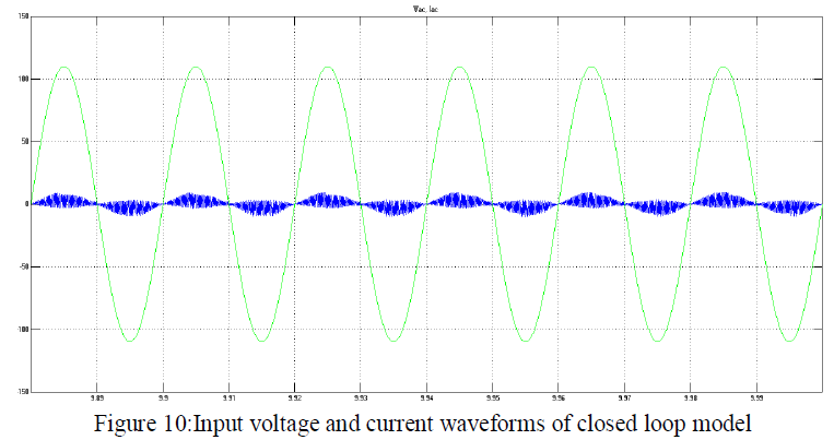
| The input voltage and current waveforms for closed loop bridgeless cuk converter is inphase and also the input current follows the input voltage waveform |
 |
| The output voltage obtained for closed loop bridgeless cuk converter is 48V and it is stabilized at 48V even when the input voltage varies in the range of 80-130V. |
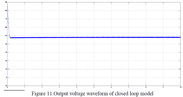 |
| The input voltage and current waveforms for the closed loop model is shown in Figure 10. The output voltage waveform for an input voltage of 110V is also shown in Figure 11. |
CONCLUSION |
| A single phase AC to DC bridgeless CUK rectifier is discussed and simulated. Performance of the converter is verified by simulation and experimental results. The bridgeless CUK rectifier is simulated in MATLAB/SIMULINK in both open loop mode and closed loop mode. The average current mode control strategy is used for the proposed circuit to improve the input power factor and to stabilize the output voltage. The closed loop model gives a power factor approximately equal to 0.999. |
References |
|