International Journal of Advanced Research in Electrical, Electronics and Instrumentation Engineering
ISSN ONLINE(2278-8875) PRINT (2320-3765)
ISSN ONLINE(2278-8875) PRINT (2320-3765)
Kumar K1, S.V. Sivanagaraju2, Rajasekharachari k3
|
| Related article at Pubmed, Scholar Google |
Visit for more related articles at International Journal of Advanced Research in Electrical, Electronics and Instrumentation Engineering
This paper presents a single stage AC-DC step up power converter that avoids the bridge rectification and directly converts the low AC input voltage to the required high DC Output voltage at a higher efficiency. In order to convert AC-DC we need a bridge rectifier and boost converter for step up the DC output voltage to meet the load demand. This twostage conversion process increases the converter cost and reduces the efficiency of converter due to presence of more no. of semi conductor devices. The proposed converter consists of a boost converter in parallel with a buck–boost converter. Boost converter operated in the positive half cycle and buck-boost converter in the negative half cycle. As a result we obtain a high DC output voltage from a low AC input voltage in single stage conversion. The proposed converter has been designed by using MATLAB.
Keywords |
| AC-DC converter, boost converter, buck-boost converter. |
INTRODUCTION |
| Power electronics may be defined as the subject of applications of solid state power semiconductor devices (Thyristors) for the control and conversion of electric power. Based up on our requirement we can control and convert electrical power by using this power electronics devices. |
A. Rectifier |
| A rectifier is an electrical device that converts alternating current (AC), which periodically reverses direction, to direct current (DC), current that flows in only one direction, a process known as rectification. Rectifiers have many uses including as components of power supplies and as detectors of radio signals. Rectifiers may be made of solid state diodes, vacuum tube diodes, mercury arc valves, and other components. A device which performs the opposite function (converting DC to AC) is known as an inverter. When only one diode is used to rectify AC (by blocking the negative or positive portion of the waveform), the difference between the term diode and the term rectifier is merely one of usage, i.e., the term rectifier describes a diode that is being used to convert AC to DC. Almost all rectifiers comprise a number of diodes in a specific arrangement for more efficiently converting AC to DC than is possible with only one diode. Before the development of silicon semiconductor rectifiers, vacuum tube diodes and copper (I) oxide or selenium rectifier stacks were used. |
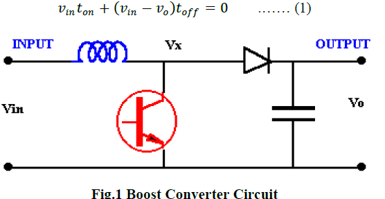
B. Boost Converter |
| The schematic in Fig. 1 shows the basic boost converter. This circuit is used when a higher output voltage than input is required. While the transistor is ON Vx =Vin, and the OFF state the inductor current flows through the diode giving Vx =Vo. |
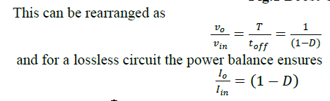
| For this analysis it is assumed that the inductor current always remains flowing (continuous conduction). The voltage across the inductor is shown in Fig. 2 and the average must be zero for the average current to remain in steady state |
 |
 |
 |
| Since the duty ratio "D" is between 0 and 1 the output voltage must always be higher than the input voltage in magnitude. The negative sign indicates a reversal of sense of the output voltage. |
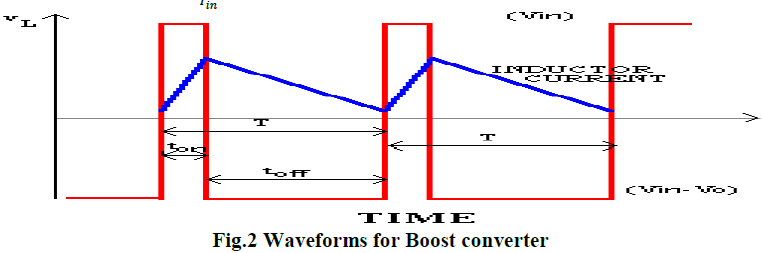
C. Buck-Boost Converter |
 |
| With continuous conduction for the Buck-Boost converter Vx =Vin when the transistor is ON and Vx =Vo when the transistor is OFF. For zero net current change over a period the average voltage across the inductor is zero. |
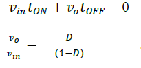 |
| Which gives the voltage ratio |
| And the corresponding current |
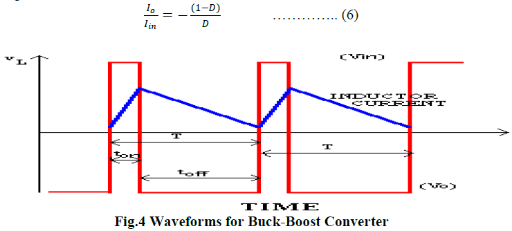 |
| Since the duty ratio "D" is between 0 and 1 the output voltage can vary between lower or higher than the input voltage in magnitude. The negative sign indicates a reversal of sense of the output voltage. |
OVERVIEW OF THE SYSTEM |
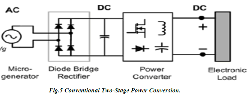 |
| The fig.5 shows the conventional two-stage method micro-generator output is given as input to the diode bridge rectifier, which converts AC to DC and stored in capacitor. Now the DC output is given as input to the power converter which boosts the input voltage. As the number of stages increases it increases the losses and reduces the converter efficiency. |
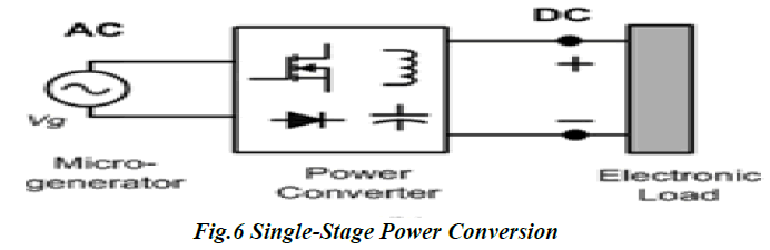 |
| In order to overcome the above drawbacks a single stage AC-DC step up converter is proposed, as shown in fig.6 it consists of a boost converter in parallel with a buck–boost converter. Boost converter operated in the positive half cycle and buck-boost converter in the negative half cycle. |
PROPOSED CONVERTER |
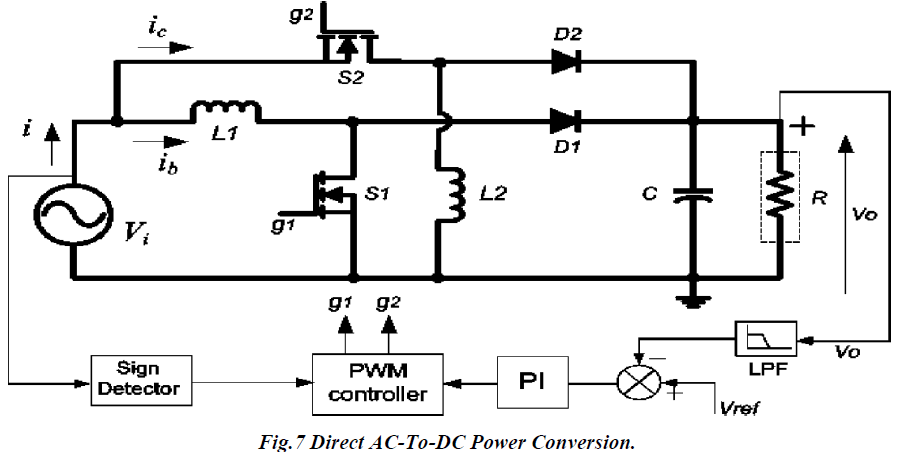 |
| A direct ac-to-dc converter is proposed. The proposed converter, as shown in Fig. 7, consists of a boost converter (inductor L1 , switch S1 , and diode, D1 ) in parallel with a buck– boost converter (inductor L2 , switch S2 , and diode D2 ). In this converter, the negative output to input voltage gain of a buck– boost converter is utilized to step-up the negative half input voltage of the micro generator to a positive high-dc output voltage. |
| The output dc bus is realized by using a single capacitor. The output capacitor is charged by the boost converter in the positive half cycle and by the buck–boost converter in the negative half cycle. Therefore, it resolves the problems present in a dual-polarity boost converter. |
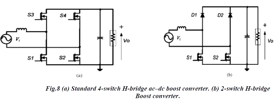
| The standard 4-switch H-bridge converter or the 2-switch H-bridge converter, as shown in Fig. 8(a) and (b) respectively, can be used for the direct ac-to-dc boost conversion. It can be noted that to achieve the boost operation, the lower switches (S1 and S2) of these two converters should be able to conduct in both the directions. In this case, without increasing the number of devices, the bidirectional conduction capability of the two MOSFETs (S1 and S2) can be used to achieve the boost operation. During the positive half cycle of the input voltage, S2 is kept ON for the entire half cycle and the gate pulse to S1 is controlled to achieve the boost operation. Likewise, in the negative half cycle, S1 is kept ON for the entire half cycle and S2 is controlled. To achieve the boost operation, these two topologies use single inductor compared to the two inductors used in the proposed converter in this study (see Fig. 7). However, there are several disadvantages in these two H-bridge converters. First, in these converters, there are two devices in the conduction path during charge or discharge of the boost inductor. |
| In the proposed converter, only a single device conducts during the charge or discharge of the inductors. In the converter, proposed in this paper, any MOSFET is operated only for a half cycle of the input ac voltage, whereas, in the H-bridge-type converters, the MOSFETs, used for the boost operation (S1 and S2), are operated for the entire cycle of the input ac voltage. Therefore, the device conduction losses in the proposed converter are reduced by more than a factor of two. In energy harvesting applications, as the power level is very low, these losses are significant compared to the total output power. |
| Second, as the MOSFETs are designed for forward conduction, in the reverse conduction mode they offer higher ON-state resistance. |
 |
| This further increases the conduction losses in the H-bridge topologies. Third, the input voltage polarity has to be sensed to control S1 and S2, but in the H-bridge topologies, the input voltage source is floating with respect to the output voltage ground. Therefore, the implementation of the control circuit is difficult. This can be easily implemented in the proposed converter. Furthermore, it can be mentioned that although the proposed converter uses two inductors (L1 and L2), they do not operate in the same half cycle. Therefore, their total losses are almost equal to the losses of the single inductor used in the H-bridge converters. |
SIMULATION CIRCUIT |
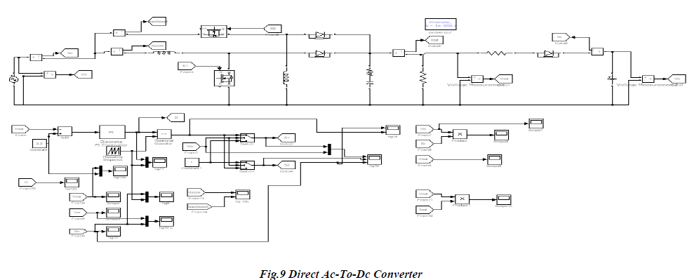
| The proposed direct ac-to-dc power conditioning circuit, as shown in Fig.9, consists of one boost converter in parallel with one buck–boost converter. The output capacitor C of this converter is charged by the boost converter (comprising inductor L1, switch S1, and diode, D1) and the buck–boost converter (comprising inductor L2, switch S2, and diode D2) during the positive half cycles and the negative half cycles of the sinusoidal ac input voltage (vi), respectively. N-channel MOSFETs are utilized to realize the switches S1 and S2. It can be noted that the MOSFETs are subjected to reverse voltage by the ac output of the micro generator. To block the reverse conduction, the forward voltage drop of the body diodes of the MOSFETs is chosen to be higher than the peak of the input ac voltage. |
 |
| Two Scotty diodes (D1 and D2) with low forward voltage drop are used in the boost and the buck–boost converter circuits for low losses in the diodes. It can be mentioned that the diodes can be replaced by MOSFETs to further improve the efficiency of the converter. |
| The proposed converter is operated under discontinuous mode of operation (DCM). This reduces the switch turn ON and turn OFF losses. The DCM operation also reduces the diode reverse recovery losses of the boost and buck–boost converter diodes. |
| Furthermore, the DCM operation enables easy implementation of the control scheme. It can be noted that under constant duty cycle DCM operation, the input current is proportional to the input voltage at every switching cycle; therefore, the overall input current will be in-phase with micro generator output voltage. The converter operation can be divided mainly into four modes. Mode-1 and Mode-2 are for the boost converter operation during the positive half cycle of the input voltage. Under Mode-1, the boost switch S1 is ON and the current in the boost inductor builds. During Mode-2, the switch is turned OFF and the output capacitor is charged. The other two modes: Mode-3 and Mode-4 are for the buck–boost converter operation during the negative half cycle of the input voltage. Under Mode-3, the buck–boost switch S2 is ON and current in the buck–boost inductor builds. During Mode-4, the buck–boost switch S2 is turned OFF and the stored energy of the buck–boost inductor is discharged to the output capacitor. |
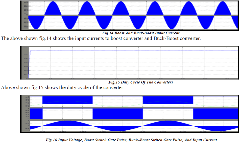
SIMULATION RESULTS |
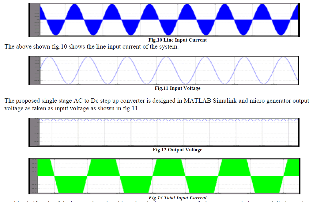 |
| Positive half cycle of the input voltage is subjected to the boost converter (inductor L1 , switch S1 , and diode, D1 ) and negative half cycle of input voltage is subjected to buck– boost converter (inductor L2 , switch S2 , and diode D2 ). The output dc bus is realized by using a single capacitor. The output capacitor is charged by the boost converter in the positive half cycle and by the buck–boost converter in the negative half cycle. As a result we obtained a step up dc output voltage as shown in fig.12. |
 |
CONCLUSION |
| The proposed single stage AC to DC step up converter is designed in MATLAB- Simulink. It avoids the conventional bridge rectification and achieves higher efficiency. The proposed converter consists of a boost converter in parallel with a buck–boost converter. The output dc bus is realized by using a single capacitor. The output capacitor is charged by the boost converter in the positive half cycle and by the buck–boost converter in the negative half cycle. Therefore, it resolves the problems present in a dual-polarity boost converter. The proposed converter uses two inductors (L1 and L2), they do not operate in the same half cycle. Therefore, their total losses are almost equal to the losses of the single inductor used in the H-bridge converters. As it consists of less number of switches and the conversion of AC to DC and boosting the input voltage is in single step as results it reduces the switching losses and conversion losses, then we obtain a high efficient single stage AC to DC step up converter. Based on the analysis, a simplified single stage AC to DC step up converter is proposed for high-voltage step-up application. |
References |
|