ISSN ONLINE(2319-8753)PRINT(2347-6710)
ISSN ONLINE(2319-8753)PRINT(2347-6710)
Anilett Benny1, Dr.T. Ruban Deva Prakash2
|
| Related article at Pubmed, Scholar Google |
Visit for more related articles at International Journal of Innovative Research in Science, Engineering and Technology
Space Vector Based Pulse Density Modulated scheme for multilevel inverter is proposed in this paper. A two level and three level inverters with three different DC input voltages are used to produce 18 stepped output sinusoidal voltage. First order sigma delta modulator is used to obtain Pulse Density Modulation. The vector space is divided into 18 segments for spatial quantization. Sixty degree co-ordinate system is used to avoid fractional arithmetic. The proposed scheme uses only switching vectors which lie on the vertices of 18 sided polygon. The scheme uses only sector identification for selecting the switching vectors without using lookup table and timer. The proposed scheme with 18 sided polygonal multilevel inverter results in elimination of 5th, 7th, 11th and 13th order harmonics when compared to two level inverter schemes. Simulation results of the proposed scheme are compared with that of two level inverter schemes. From the results, the total harmonic distortion (THD) of the output voltage of SVPDM based 2-level inverter is 31.13% and the 18-sided multilevel inverter with SVPDM is 10.11%. From the results, the validity of the SVPDM based 18-sided multilevel inverter has been confirmed. Zero voltage switching can be incorporated in future for achieving high efficiency
Keywords |
| Space vector pulse density modulation, multi-level inverter, two level inverter, harmonics, sigma delta modulator. |
INTRODUCTION |
| Pulse density modulation (PDM) control method is applied in order to reduce the switching loss of the inverter side. In this method the density and the plus/minus of the constant width pulse is controlled, and then these pulse signals are used as switching pulses [5]. In general, delta-sigma conversion is used for analog-digital conversion. These PDM signals are used to turn on/off the inverter arm in PDM inverters. Delta-sigma conversion generates the inverse voltage pulses in order to cancel the quantization error. In order to resolve this problem, the PDM based SVM is proposed [6]. In PDM based SVM, the phase error between the voltage and current does not occur rapidly, because the SVM controller can select the switching pattern and hence the phase change on the voltage becomes smaller. Space vector based pulse density modulation (SVPDM) is proposed for two-level inverters. The total harmonic distortion in 2-level inverter is large. Multilevel inverters have become more superior to conventional two level voltage inverters [1][2]. Different topologies of multilevel inverters are explained in literature [3], [7], [10]. SVPWM is commonly used [8] for generating switching pulses where the switching losses are more. Hence we propose SVPDM for multilevel inverter. Pulse density modulation scheme consists of a first order delta sigma modulator and a space vector quantizer [4]. 12-sided polygonal voltage space vector concept for PWM is proposed in [9]. In this paper, the principle of vector quantization is applied for 18 sided polygonal voltage space vector. A two level inverter and a three level inverter feeding both ends of a load are used to produce the stepped output voltage. Three level inverter is made by cascading two 2 level inverters fed with asymmetrical voltages. The advantage of using multilevel inverters is the reduction of EMI and harmonics. Also the power circuit can be realised with low voltage devices and can be operated with low switching losses. The proposed 18 sided polygonal voltage space vector structure gives an increased modulation range with the absence of 5th, 7th, 11th and 13th harmonics from the output voltage [7]. So this scheme can be considered as available alternative for low and medium voltage high power drive applications. |
II. SPACE VECTOR PULSE DENSITY MODULATION SCHEME |
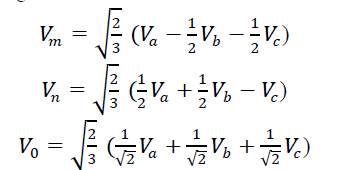
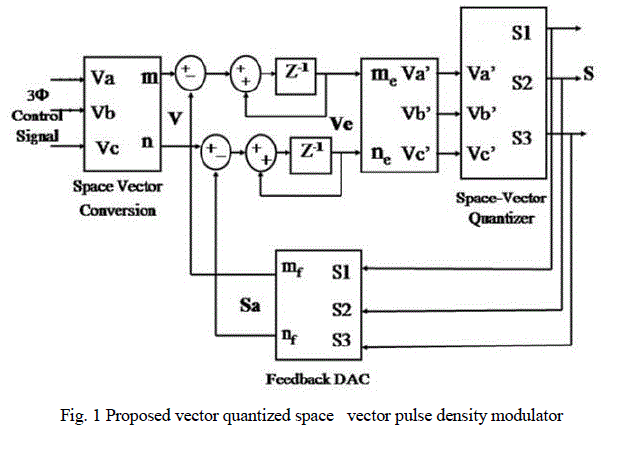
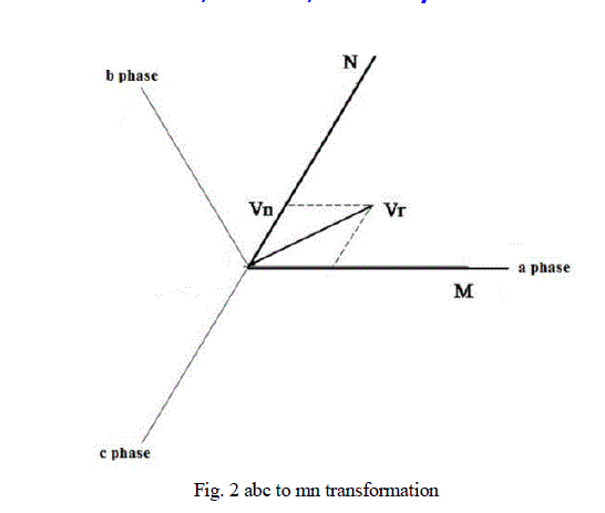
| Fig. 1 represents proposed space vector pulse density scheme for multilevel inverter with 18 sided polygonal voltage space vector. The instantaneous values of three phase voltages are converted into reference voltage space vector Vref. The instantaneous values are resolved into sixty degree (m-n) coordinate system (Fig. 2). The m-axis is placed along A phase. The transformation equations are given below: |
 |
| Each forward path consists of a first order sigma delta modulator consisting of a difference node, discrete time integrator, a quantizer and a digital to analog converter. The space vector quantizer consists of two parts, m-n to three phase voltage converter and a space vector quantizer. The difference between reference space vector Vref and analog estimate of quantizer output vector Sa is integrated to obtain error vector Ve in delta sigma modulator. The error vector is quantized to obtain switching sectors S. The m-n frame components are converted back to three phase voltages. |
 |
 |
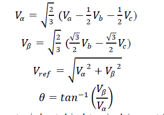
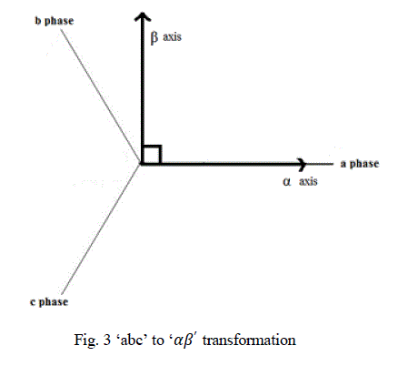
| In space vector quantizer the three phase components are again converted to ïÿýïÿýïÿýïÿý frame components (Fig.3) to produce the reference voltage vector and angle of sector selection using the transformation equations given below: |
 |
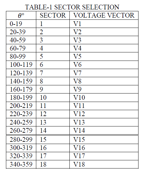
| The sector in which the voltage space vector is located is determined (as per table-1) for finding out the multilevel inverter switching states. |
 |
| The output voltage is fed back and converted to m-n frame components. The m and n components are added to delta sigma loop as shown in the figure. |
 |
III. MULTILEVEL INVERTER WITH 18 SIDED POLYGONAL VOLTAGE SPACE VECTOR |
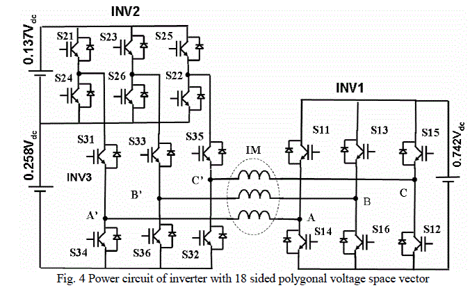
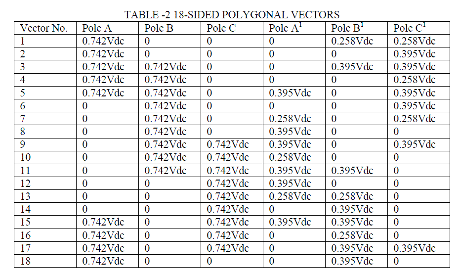
| Multilevel inverter to generate 18-sided polygonal voltage space vectors is shown in Fig.4. It consists of a 2-level inverter on one side and a 3-level inverter on the other side of load. The 3-level inverter is made by cascading two conventional 2-level inverters. Asymmetrical DC link voltages are used for the inverters. For the proposed inverter we can achieve 6 different voltage levels in each winding. Therefore a total of 63 =216 switching states can be generated. Out of these switching states, vectors which lie on the vertices of 18 sided polygon are selected to generate 18-sided voltage space vector. Each pole A, B or C in INV1 can be independently connected either to 0.742Vdc or to the zero voltage. The poles A1, B1 or C1 of INV2 can be connected to any of three levels 0, 0.258Vdc or 0.395Vdc independently. This can be used to generate 18 polygonal voltage space vectors. The top and bottom switches in each leg of the inverter compliments to each other. The state of upper switch determines the state of lower switch. |
 |
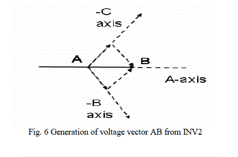
| The 18 voltage space vectors are shown in Fig.5. The angle between two adjacent voltage vectors is 20°. Resultant sum of vector OA and AB gives vector 1. In first segment INV1produces vector OA by connecting the pole A to 0.742Vdc. Vector AB has a magnitude of 0.258Vdc and is generated as shown in the Fig. 6. Pole voltages A1, B1, and C1 of INV2 are subtracted from the pole voltages A, B, C of INV1. When B1 is connected to 0.258Vdc it is along the negative B-axis and when C1 is connected to 0.258Vdc it is along the negative C-axis. Their resultant is AB with magnitude 0.258Vdc along A-axis. The vectors AB and OA gives vector 1 of magnitude Vdc. |
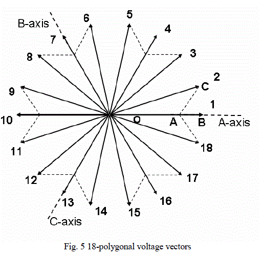 |
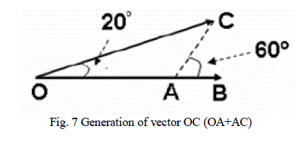
| In the second sector, pole A of INV1 is connected to 0.742Vdc, poles B and C at zero level. Hence vector OA is produced. Pole voltages A1 and B1 are at zero voltage levels and C1 at 0.395Vdc. Vector sum of the above vectors yields vector 2 in Fig. 7. Vector-3 is generated as follows. In INV1 pole voltages A and B are maintained at 0.742Vdc, while C is at 0Vdc. Hence a vector is produced along the negative C-axis with a magnitude equal to 0.742Vdc. In INV2 pole A1 is at zero level while B1 and C1 are at levels 0.395Vdc. This produces a vector with magnitude of 0.395Vdc along the positive A axis. Together the vector sum produces vector 3 in Fig.5. |
 |
 |
 |
IV. SECTOR IDENTIFICATION |
| The angle calculation in space vector quantizer is used to identify the sector. Depending upon the value of angle calculated in ïÿýïÿýïÿýïÿý frame, one of the 18 sectors is selected and switching vector corresponding to that specific sector is applied to multilevel inverter. |
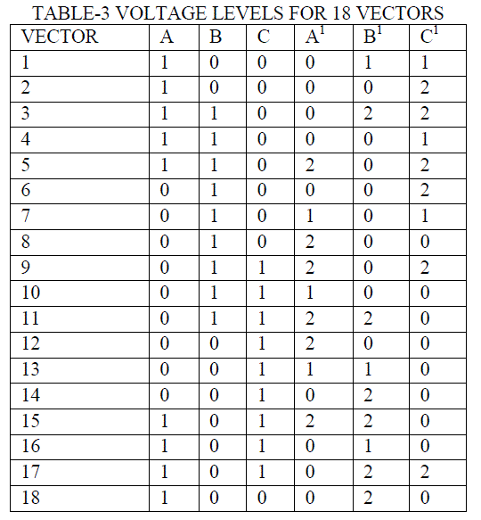 |
| Voltage level in A, B, C: 0=0 & 1=0.742Vdc; Voltage level in A1, B1, C1: 0=0, 1=0.258Vdc & 2=0.395Vdc |
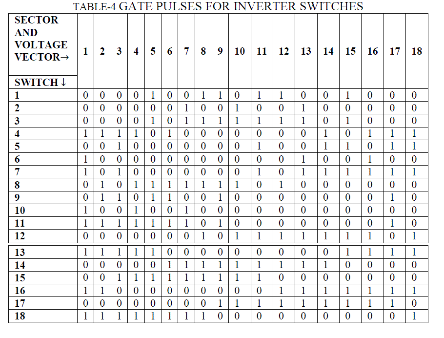 |
| Gate pulses for each inverter switches are generated individually by calculating the voltage levels for each vector from table-3. Hence sector identification is performed. The switching pulses for inverter switches are shown in table-4. |
V. SIMULATION RESULTS |
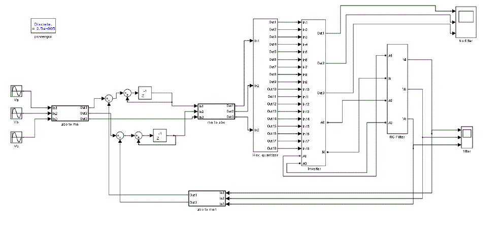
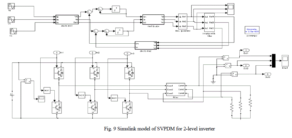
| The simulink model of the proposed SVPDM scheme for 18-sided multilevel inverter is shown in Fig.8. The inverter sub system is also shown in the figure. The simulink model of SVPDM for two-level inverter is shown in Fig.9. |
 |
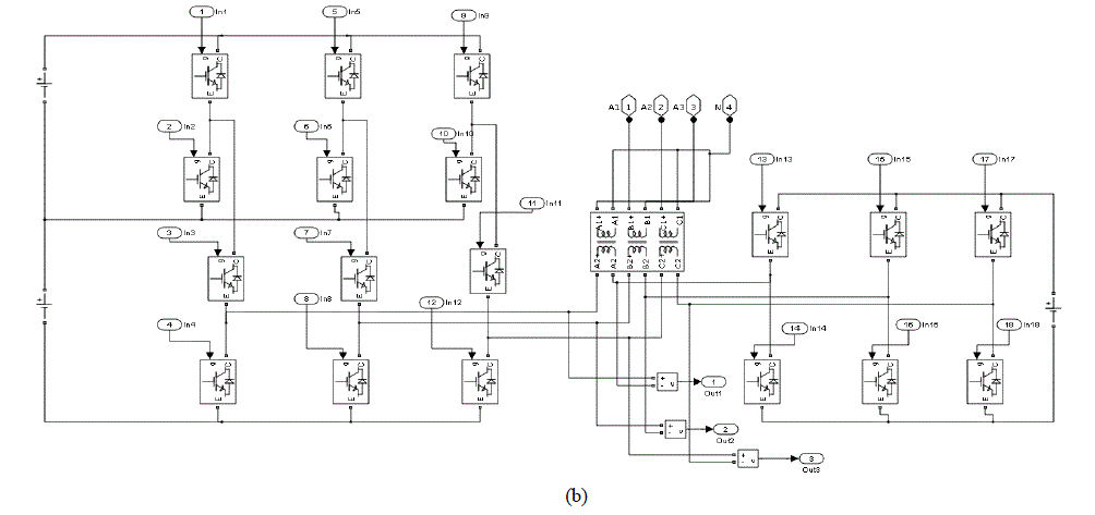 |
| Fig. 8 Simulink model (a) Main model (b)18-sided multilevel inverter subsystem |
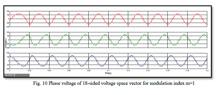
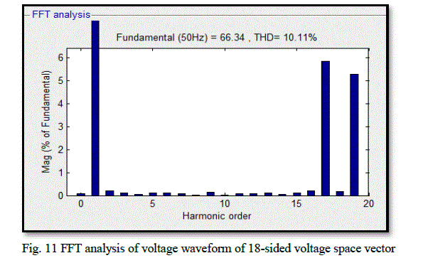
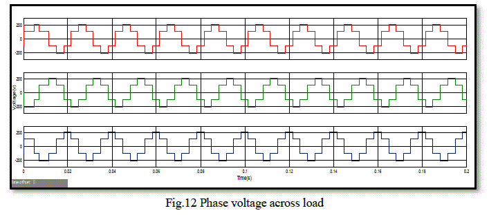
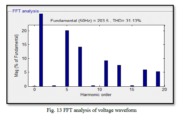
| The phase voltage of 18-sided voltage space vector and its FFT analysis are shown in Fig. 10 and Fig. 11. The total harmonic distortion is found to be 10.11%. The phase voltage of two-level inverter with hexagonal quantizer and its FFT analysis are shown in Fig. 12 and Fig. 13. The total harmonic distortion is found to be 31.13% From simulation results it is found that the phase voltage for multilevel inverter with 18 sided voltage space vector produces 18 stepped output waveform. For a two level inverter with hexagonal quantizer, the phase voltage is 6- stepped waveform. When harmonic analysis is performed, the proposed scheme with multilevel inverter is found to eliminate 5th, 7th, 11th and 13th order harmonics. The Total Harmonic Distortion (THD) factor for the proposed scheme is very less when compared with the two-level inverter with hexagonal quantizer. |
 |
 |
 |
 |
 |
V. CONCLUSION |
| An 18-sided multilevel inverter control scheme using space vector pulse density modulation is proposed. Sigma delta modulation and vector quantization principles are used in this scheme. The vector space is divided into 18 segments for spatial quantization. Sixty degree co-ordinate system is used to avoid fractional arithmetic. The proposed scheme uses only switching vectors which lie on the vertices of 18 sided polygon. The scheme uses only sector identification for selecting the switching vectors without using lookup table and timer. Simulation studies are performed for SVPDM based 2-level and multilevel inverter with 18-sided voltage space vectors. Pulse density modulation scheme for multilevel inverter with 18 sided voltage space vector yields low switching losses and very less harmonic content as compared to pulse width modulation techniques in multilevel inverters. The proposed scheme can be implemented for multilevel inverter with 12 sided voltage space vectors. Zero voltage switching can be incorporated in future for achieving high efficiency. This scheme is simple and timing calculations for voltage vectors are eliminated. |
References |
|