International Journal of Advanced Research in Electrical, Electronics and Instrumentation Engineering
ISSN ONLINE(2278-8875) PRINT (2320-3765)
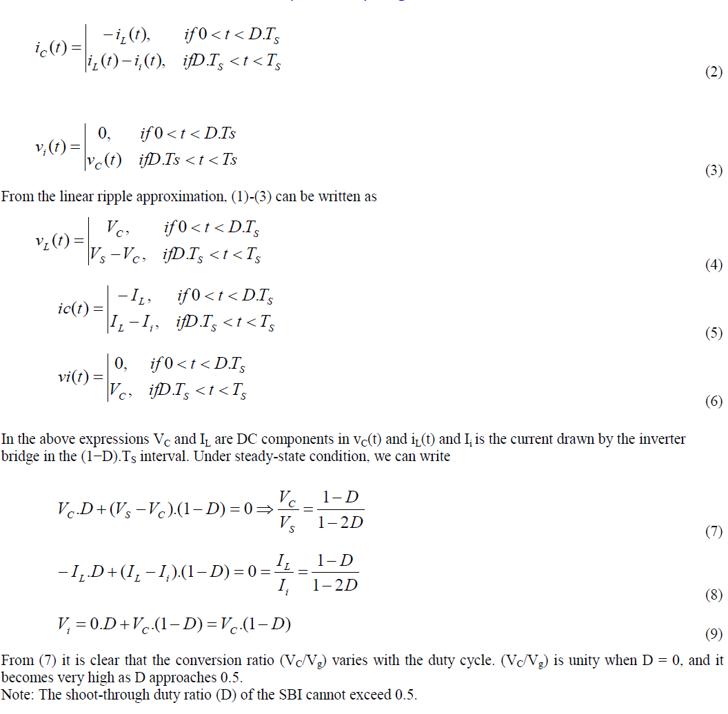
ISSN ONLINE(2278-8875) PRINT (2320-3765)
Shilpa A. S1., H. Vasantha Kumar Shetty2
|
| Related article at Pubmed, Scholar Google |
Visit for more related articles at International Journal of Advanced Research in Electrical, Electronics and Instrumentation Engineering
The objective in this paper is to study the operating modes and analysis of the Switched Boost Inverter (SBI). The performance of the proposed SBI is similar to that of Z-Source Inverter (ZSI). In comparison to the ZSI, the present topology results in lower volume and lower cost since it reduces the number of passive component. This feature makes it more suitable for low power applications than ZSI. For the proper operation of the inverter, with special consideration to its operating principle (shoot-through i.e., conduction of two switches on the same leg of the inverter), a modified PWM control strategy is also described in detail. In addition, mathematical relations between various performance parameters under this modified PWM technique have been described in detail. Simulation is carried out using Matlab/Simulink software to verify the theoretical analysis made. This report also presents a laboratory prototype of the Switched boost inverter along with it results.
Keywords |
| Z-Source Inverter, Switched Boost Inverter, Modified PWM technique, Shoot-through, Non-Shootthrough. |
INTRODUCTION |
| ZSI employs a unique impedance network to couple the converter circuit to the power source, thus providing unique characteristic features that cannot be found in the traditional Voltage source inverter and Current source inverter. The unique impedance network mentioned above, implements two capacitors and two inductors. Introduction of these passive components add weight and size to the whole inverter. In order to reduce size and weight, a new topology is considered which involves lesser passive components, meanwhile trying to attempt similarity in all the steady state performance. This new topology is called Switched Boost inverter, which is being studied and analysed in this report. |
II. LITERATURE SURVEY |
| The basic idea of SBI [2] is derived from ZSI [1]. By controlling the shoot-through duty cycle, the ZSI can be able to produce any AC output voltage from a given DC input voltage. This feature makes the ZSI suitable for number of applications such as renewable power systems (photovoltaic and fuel cells), adjustable speed drives, general purpose motor drives, electric vehicles, uninterruptible power supplies [3]-[8] etc. |
| Conventional pulse-width modulation techniques can be modified strategically to affect the operation of ZSI continuously or discontinuously, while retaining all the harmonic performance features of the conventional modulation techniques [9]. The complete analytical performance of the ZSI using X-shaped LC impedance network is complicated. Hence a small signal model method is resorted in [10] to derive transfer function and asses the performance there upon. From literature survey it is evident that ZSI is a promising technology for both buck and boost operations. But ZSI has the drawback of employing more and bulky passive components. Therefore SBI topology has been proposed [2] to reduce the number of passive components, thus can be used in low power applications where size and weight matters. |
II.SWITCHED BOOST INVERTER |
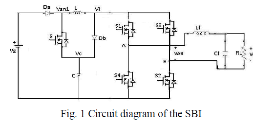
| Fig. 1 shows the schematic arrangement of the SBI, which is a buck-boost type of DC-AC converter just like the classical ZSI. The major components like active switch(S), two diodes (Da, Db), one inductor (L), and one capacitor (C) are interposed between voltage source, Vg and the inverter bridge. These components form the switched boost network of the SBI. A low pass filter is used at the output of the inverter bridge to filter the switching frequency components in the output voltage of H-bridge, VAB. Lf and Cf form the filter circuit. RL is the load. Vo is the final output of the inverter bridge after filtering the switching frequency components in VAB. |
| The circuit of SBI makes use of the MOSFET switches S, S1, S2, S3 and S4. However, one can also think of IGBT version with proper integration of the gate circuit. Vsn1 denotes switch node-1 voltage and Vi denotes the switch node-2 voltage or inverter input voltage or DC link voltage. VC is the capacitor voltage. |
| In order to analyse the steady state characteristics of SBI, consider TS be one switching cycle time (time taken to finish one complete cycle) and the D be the duty cycle (amount of time the signal is in a high state as a percentage of the total time it takes to complete one cycle). |
 |
| For the of steady-state analysis, the operating states are divided into shoot-through and non-shoot-through states. Initially, the inverter is assumed to be in shoot-through state for duration D.TS during switching cycle TS. The switch S is turned on during this interval. The inverter bridge is shorted through upper and lower switching devices in the phase legs. The equivalent diagram is as shown in Fig. 2a. During the shoot-through state, the inverter bridge will be short circuited. Diodes Da and Db are reverse biased as VC >Vg. Capacitor C charges the inductor L through switch S and the inverter bridge. The inductor current in this interval equals the capacitor discharging current. |
| For the remaining duration in the switching cycle i.e., (1 −D).TS, the inverter will be in non-shoot-through state. The switch S is turned off. In this interval the inverter bridge is represented by a current source as shown in Fig. 2b. During the non-shoot-through, the Vg and L together supply power to the inverter and the capacitor through Da and Db. The inductor current in this interval equals to the sum of capacitor charging current and the inverter input current. |
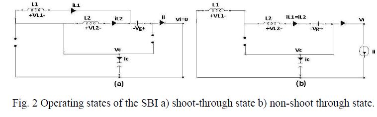 |
| Referring to the Fig. 2a and Fig. 2b we can write the following expressions. |
 |
 |
III. PWM CONTROL OF SWITCHED BOOST INVERTER |
| modified PWM control strategy [2] is used for the proposed SBI based on the traditional sine-triangle PWM. In this scheme the switching losses have been reduced and here the switching frequency of S is always constant. vtri (t) is a high frequency triangular carrier of amplitude VP and having frequency fs. vm(t) and −vm(t) are the sinusoidal modulation signals of amplitude M.VP (M is the modulation index) and having frequency fo. The fs is chosen such that, it is much greater than the fo. Due to this reason, vm(t) is nearly constant during a switching cycle. |
| The signals ST1 and ST2 are generated by comparing vtri (t) with constant voltages, VST and −VST respectively. The gate control signals for switch S1 (GS1) and switch S2 (GS2) are generated by comparing vm(t) and −vm(t) with vtri (t). The gate control signals for switch S3 (GS3) is generated by NAND operation on ST1 and GS2 and the gate control signals for switch S4 (GS4) are generated by NAND operation on ST2 and GS1. The gate control signals for the switch S (GS) are generated by NAND operation on ST1 and ST2. Inverter input voltage will be high when GS is low and vice-versa. |
| The following relations have been established for the proper operation of the SBI using modified PWM technique. |
| 1. Relation between constant voltage (VST) and shoot-through duty ratio |
 |
IV.RESULTS AND DISCUSSION |
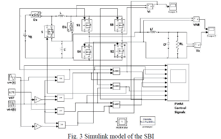
| Simulation is carried out using Matlab/Simulink software. The simulink model is as shown in Fig. 3. Modified PWM technique has been used here. VST is a constant, whose value is 0.75. Multimeter is used to measure the voltage across the capacitor C. Refer Chapter 3 for the details of the modified PWM technique employed in SBI. |
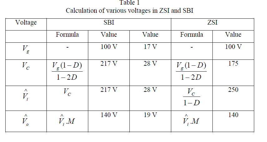
| Calculations of various voltages in SBI are shown in Table 1. Two sets of calculations have been made, keeping the duty cycle same but with different input voltage and different modulation index. The first set is intended for the comparison of SBI with that of ZSI. Input voltage considered in the first set is high i,e 100 and M=0.48. The second set is used to verify the hardware results. Input voltage considered in second set is less i,e 17 V and M=0.63. The switching frequency is 10 kHz and D=0.3 in both the cases. In the simulation, all of the components are assumed ideal. L=5mH, C=100μF and RL= 1kΩ. The following waveforms are obtained: |
 |
 |
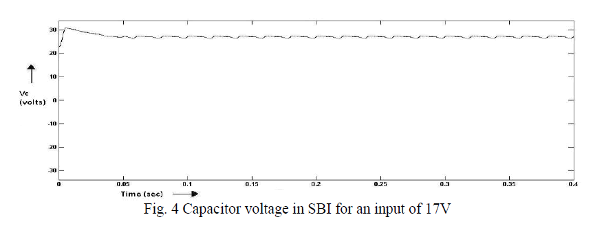 |
| Fig. 4 shows the voltage across the capacitor in SBI. The capacitor voltage is boosted to nearly 1.7V times the input voltage in steady state i.e., 28V. In case of SBI, the capacitor voltage is equal to the inverter input voltage. So the input voltage to the inverter is also boosted nearly 1.7 times the input voltage. |
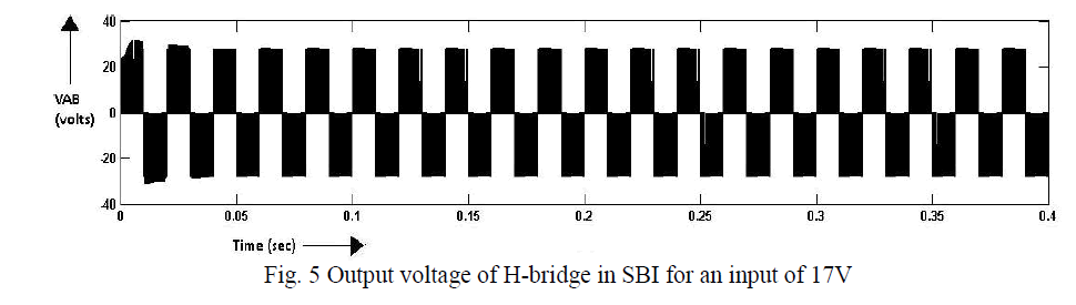 |
| Fig. 5 shows the output voltage of H-bridge in SBI. The VAB is 29V. The output of the H-bridge is usually a square wave. To make this into sine wave output, a low-pass LC filter is used on the output side of the inverter. |
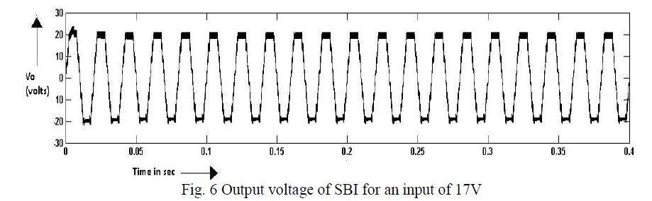 |
| Fig. 6 shows the inverter output voltage after filtering the switching frequency components in the output voltage of Hbridge. The output voltage is 19 V. The waveforms obtained through SBI simulation do confirm the mathematical analysis made in Table 1 |
V. EXPERIMENTAL VERIFICATION |
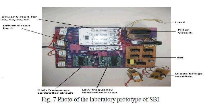
| The photograph of the SBI prototype is shown in Fig. 7. The prototype is explained by dividing the entire setup into three functional blocks. The first is the controller circuit, the second is the gate driver circuit and the third is the main SBI circuit. |
 |
| The controller circuit gives the control signals which operate the gate driver circuit. The gate driver circuit will drive the respective switches of the SBI circuit. The working of each circuit is explained in detail as below: |
| 1.Controller circuit: The AT89S52 is a low-power, high-performance CMOS 8-bit microcontroller. It is a very popular, low cost, general purpose microcontroller due to their industry standard instruction set. There are two controller circuits. One is used for high frequency i.e., for controlling the main switch, S. The other is used for low frequency control i.e., for controlling other switches S1, S2, S3 and S4. |
| 230 V AC will be stepped down to 12V AC using step-down transformer. The 5V AC will be rectified and regulated by the rectifier and regulator provided on the controller circuit. The resulting 5V DC will be given as input to the controller IC. Controller IC i.e., AT89S52 will provide an output of 5 V pulse. The 5V pulse will be fed to the buffer IC of the gate driver circuit. |
| 2.Gate driver circuit: 5V pulse from the controller IC will be strengthened using the buffer amplifier i.e., the current will be increased but the voltage remains the same. The output of the buffer amplifier is 5V dc. The output of the buffer IC will be given as the input to the opt coupler IC. An opto-isolated gate driver is used in order to provide isolation between the low power controller circuit and the main SBI circuit. Due to the opto-isolation, signals strength may deteriorate. To overcome this, TTL (Transistor Transistor Logic) and transformer combination is used. Generally speaking, TTL use NPN and PNP type bipolar junction transistors. |
| 3. SBI circuit: 230V AC is stepped down to 12V AC using a step-down transformer. Output of the transformer is rectified using diode bridge rectifier and rectified DC voltage is fed as input to the SBI circuit. The SBI output voltage is measured across the load RL. Outputs are obtained using the laboratory prototype of the SBI shown in Fig. 8. The result of the laboratory prototype is used to verify the theoretical analysis simulation results. |
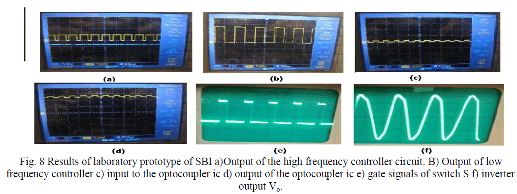 |
| Fig. 8a shows the output of the high frequency controller. The output is obtained at Pin. 1 of high frequency controller IC. As mentioned earlier the output of the controller IC is a 5V pulse. Its frequency is 10 kHz. Fig. 8b shows the output of the low frequency controller. The output is obtained at Pin. 1 of low frequency controller IC. In case of low frequency controller IC also the output is a 5V pulse. But as its name says the frequency is less. Its frequency is 50 Hz. Fig. 8c shows the input to the opt coupler IC. The input voltage here is very less i.e., 1.2 V. The optocoupler stage provides isolation between the low power controller circuit and the main SBI circuit. Due to the opto-isolation, signals strength may deteriorate. To overcome this, TTL and transformer combination is used. Fig. 8d shows the output of the optocoupler IC. Compared with the input stage the output signal strength has been increased it is due to the TTL logic implemented. Signal has a magnitude of around 15V here. This signal is used to the turn on the switches of SBI. Fig. 8e shows the gate control signals of switch S. The switching frequency here is high i.e., 10 kHz. It operates at a duty cycle 0.3 as shown. Whenever the gate signal to the S is high i.e., GS is high, the Vi will be low and vice-versa. Fig. 8f shows the inverter output voltage. For a given input voltage of 17V, the output has been boosted to 18.5 V. |
VI COMPARISON OF SBI AND ZSI |
| 1. Comparison of the Boost Ability: The peak dc-link voltage across the inverter circuit, to the dc input is termed as the boost factor. The boost factor for the SBI (BSBI)and ZSI (BZSI)can be given by |
 |
| The boost ability of the SBI inverter is lesser than than that of ZSI[1] and SBI. |
| 2. Comparison in terms of Voltage conversion ratio versus Modulation index: The voltage conversion ratio for SBI (GSBI) and ZSI (GZSI) can be given as: |
 |
| Compared with the ZSI using the same modulation index, the SBI provides a higher voltage boost inversion. Therefore, for the same gain, the SBI use a higher modulation index in order to improve the inverter output quality. |
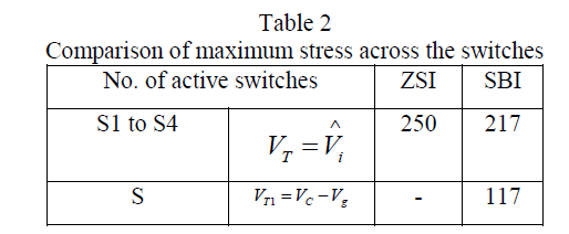
| 2. Comparison of maximum voltage stress: Table 2 lists the maximum voltage stress across the switches for ZSI and SBI. It shows that the SBI provides a lower voltage stress across the active switches. |
 |
| 4. Comparison of number of components: The SBI uses two passive components and three semiconductor switches, while ZSI uses four passive components and one semiconductor switch. Due to the less number of passive component, the SBI may lead to reduction in the size and weight of the overall power converter when compared to a ZSI. But increases in the number of semiconductor devices, the SBI requires a better protection circuit when compared to ZSI. |
References |
|