International Journal of Advanced Research in Electrical, Electronics and Instrumentation Engineering
ISSN ONLINE(2278-8875) PRINT (2320-3765)
ISSN ONLINE(2278-8875) PRINT (2320-3765)
Jaspreet Kaur1, Harpreet Kaur2
|
| Related article at Pubmed, Scholar Google |
Visit for more related articles at International Journal of Advanced Research in Electrical, Electronics and Instrumentation Engineering
Reversible logic circuits have emerged as a promising technology having its applications in low power CMOS, Quantum Computing, nanotechnology, and optical computing. Power is the major constraint for any circuit Each circuit demands not only low power, but fast speed. This paper is focused on the efficient design of the full Adder/Subtractor with the help of half adder subtractor with single control line The proposed design offers the efficient Adder/Subtractor in terms of gate count, garbage outputs, constant inputs and Quantum Cost. A new reversible gate COG gate is used for designing of Full adder /Subtractor. The proposed circuits will simulate in Xilinx8.2i and by writing the Code in VHDL HDL.
Keywords |
| Reversible Gates, power, Garbage output, Quantum Cost, Full adder/Subtractor. |
INTRODUCTION |
| Reversible logic has received great attention in the recent years due to their ability to reduce the power dissipation which is the main requirement in low power VLSI design. Quantum computers are constructed using reversible logic circuits. It has wide applications in low power CMOS and Optical information processing, DNA computing, quantum computation and nanotechnology. In 1960 R.Landauer’s demonstrated that high technology circuits and systems constructed using irreversible hardware result in energy dissipation due to information loss. A computation is called reversible if its inputs can always be deduced from its outputs. It’s only irreversible computations that must dissipate heat. One of the most important computational resources is energy. The energy consumption in computation turns out to be deeply linked to the reversibility of the computation. Reversible logic was first related to energy when Landauer [1] states that information loss due to function irreversibility leads to energy dissipation in 1961 who stated that there is a small amount of heat dissipation the circuit due to the loss of one bit of information and it would be equal to kTln2 where ‘k’ is the Boltzmann constant and T is the temperature . This principle is further supported by Bennett that zero energy dissipation can be achieved only when the circuit contains reversible gates in 1973.It was proved by Bennett [2] that the energy kTln2 would not be dissipated from the circuit if input can be extracted from the output and it would be possible if and only if reversible gates are used. |
II.LITERATURE SURVEY |
| Landauer, Rolf. [1]." Irreversibility and Heat Generation in the Computing Process". R Landauer’s showed, amount of heat generation due to loss of bit is kTlog2, and this value small but not negligible. Bennett, Charles H [2]. "Logical Reversibility of Computation". Bennett showed that this heat dissipation due to information loss can be avoided if the circuit is designed using reversible logic gates. No amount of heat would be dissipated from the system as long as the system was able to return to its initial state from its final state.Peres T Toffoli, E.Fredkin [8] [7] [6] proposed reversible logic gates.In In “Efficient adder circuits based on a conservative reversible logic gate”,[17] Bruce, J.W., M.A.Thornton, L. shivakuamaraiah, P.S. kokate and X. Li, used only Fredkin gates to construct full adder with gates cost equal to 4, 3 garbage outputs and 2 constant. In“Design of Fault Tolerant Full Adder/Subtractor Using Reversible Gates”[12]Kaur and Dhaliwal proposed the design of full Adder/Subtractor circuit using fault tolerant reversible logic gates. The design can work singly as a reversible Full Adder/Subtractor unit. It is a parity preserving reversible adder cell, that is, the parity of the inputs matches the parity of the outputs.In “Design and Synthesis of Fault Tolerant Full Adder/Subtractor using Reversible Logic Gates “Prashanth et al. [13] proposed the design of Full adder/subtractor circuit using fault tolerant reversible gates. The design can work singly as an adder/subtractor. The proposed design offers less hardware complexity and is efficient in terms of gate count, delay, constant inputs and garbage outputs compared to previous Fault tolerant Full Adder/Subtractor design.In “An Ease implementation of 4-bit Arithmetic Circuit for 8 Operation by using a new reversible COG gate”[11] Shefali Mamataj, Biswajit Das, Anurima Rahaman presented new reversible gate COG |
III.RELATED WORK |
A.Reversible Logic |
| A gate is reversible if the gate’s inputs and outputs have a one-to-one correspondence, i.e., there is a distinct output assignment for each distinct input Therefore, a reversible gate’s inputs can be uniquely determined from its outputs. A ramification of this definition is that reversible logic gates must have an equal number of inputs and outputs. If logic gates are classified according to the number of inputs and outputs, a gate with m inputs and n outputs is a (m, n) or m*n logic gate, where reversible gates must have m=n. Furthermore, a reversible gate’s output vector is a permutation of the numbers 0 to 2n -1. A gate is balanced if its output equals one for exactly one-half of its inputs. If a gate is not balanced, it is said to be unbalanced. Reversible gates are balanced. The only non trivial reversible logic gate in classical digital logic is the (1, 1) reversible gate, i.e. the inverter. This gate is very important since it does not introduce garbage outputs. A reversible gate without having constants on any of input bit realizes on all output bit only balanced functions, therefore it can realize non-balanced functions only with garbage outputs. An additional constraint of reversible logic is that the fan-out of every signal including primary inputs must be one [14]. The important parameters which play a major role in the design of an optimized reversible logic circuit are given by Kerntopf et al.[15] |
| ïÃâ÷ Constants: This refers to the number of inputs that are to be maintained constant at either 0 or 1 in order to synthesize the given logical function. |
| ïÃâ÷ Garbage’s: This refers to the number of outputs which are not used in the synthesis of a given function. These are very essential without which reversibility cannot be achieved. |
| ïÃâ÷ Gate count: The number of reversible gates used to realize the function. |
| ïÃâ÷ Flexibility: This refers to the universality of a reversible logic gate in realising more functions. |
| ïÃâ÷ Quantum cost: This refers to the cost of the circuit in terms of the cost of a primitive gate. It is calculated knowing the number of primitive reversible logic gates (1*1 or 2*2 ) required to realize the circuit. |
| ïÃâ÷ Gate levels: This refers to the number of levels in the circuit which are required to realize the given logic functions. |
| ïÃâ÷ Hardware Complexity: The hardware complexity is measured by counting the number of AND operations, number of EX-OR operations and number of OR operations. Let α = No. of EX-OR operation, β = No. of AND operations, δ = No. of NOT operations Then the total hardware complexity T is given as sum of EX-OR, AND and NOT operations.[16] |
B.Reversible Logic gates |
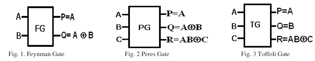
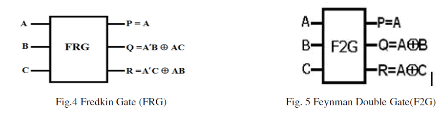
| A reversible logic gates are those which performs one to one mapping with the same number of inputs and outputs. In other words, if any reversible gate has ‘n’ no of inputs and same ‘n’ no. of outputs, then that reversible gate is also known as a n*n reversible logic gate. There exist many reversible gates in the literature. Among them 2*2 Feynman gate (FG) [5], depicted in Fig. 1, 3*3 Peres gate (PG) [6], depicted in Fig. 2, 3*3 Toffoli gate (TG) [7], depicted in Fig.3, 3*3 Fredkin gate (FRG) [8], depicted in Fig.4, 3*3 Feynman Double gate (F2G) [5], depicted in Fig.5 have been studied extensively. Because of their simplicity and low cost there are design approaches and tools that incorporate them separately or in combination with each other [9]. |
 |
 |
IV. A 4 *4 MIG REVERSIBLE GATE |
| A 4*4 reversible gate Modified Islam Gate(MIG) is already had proposed [10] shown in Fig 6.In this gate the input vector is given by A,B,C,D and output vector is given by P,Q,R,S. |
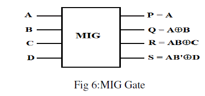 |
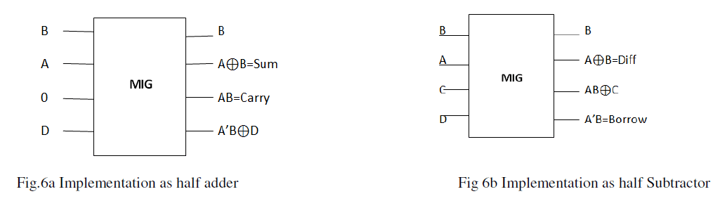
| We can mplement half adder and half Subtractor adder by using MIG gate as shown in Fig 6a and Fig 6b respectively |
 |
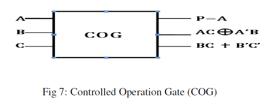
V. A 3*3 COG REVERSIBLE GATE |
| A 3*3 Controlled Operation Gate(COG) is already had proposed[11].It has three inputs A,B,C and three outputs P,Q,R.The COG is shown in Fig 7 |
 |
VI. PROPOSED WORK |
| The proposed design which consists of both adder and subtractor can work with the help of single control line. The design will consists of control line Ctrl which will selects adder or subtractor according the control logic input: |
| (i) If ctrl=0 circuit will act as Adder |
| (ii) If ctrl=1 circuit will act as Subtractor |
| This design of adder/subtractor is improved from previous designs in the terms of garbage outputs and constant inputs. The work covers the design of reversible half adder/subtractor, full adder/subtractor, 4-bit Serial adder/subtractor with COG gate. |
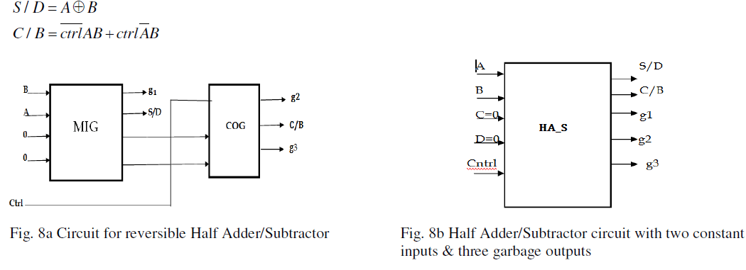
A. Design of the reversible Half Adder/Subtractor circuit (HA_S) |
| The designing of this unit can be done with the help of MIG and COG Gate. The selection of half adder/subtractor is done by control line [12]. When control signal Ctrl is at logic 0, the circuit acts as half adder & when Ctrl goes to logic 1, the circuit performs as half subtractor. The sum & difference is represented by S/D and its carry & borrow signal is represented by C/Bin Fig.8a The two inputs which are said as constants are forced to logic 0 whereas the garbage signals are g1 to g3. From Fig. 8b, it can be seen that the reversible half adder/subtractor (FTHA_S) circuit posses five inputs and correspondingly five outputs as per reversible rule.. The outputs of proposed circuit are: |
 |
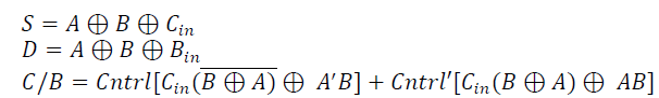
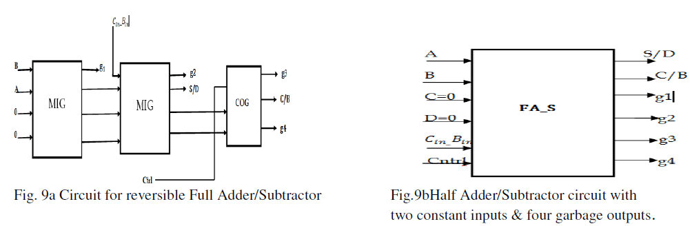
B. Design of the reversible Full Adder/Subtractor circuit (FA_S) |
| The designing of this unit can be done with the help of two MIG and COG Gate .The selection of full adder/subtractor is done by control line. When control signal ctrl is at logic 0, the circuit acts as full adder & when ctrl goes to logic 1, the circuit perform as full subtractor [13]. The sum & difference is represented by S/D and its carry & borrow signal is represented by C/B in Fig.10. The rest four inputs which are said as constants are forced to logic 0 whereas the garbage signals are g1 to g3. From Fig. 11, it can be seen that the reversible half adder/subtractor (FTHA_S) circuit posses Six inputs and correspondingly Six outputs as per reversible rule.. The outputs of proposed circuit are: |
 |
 |
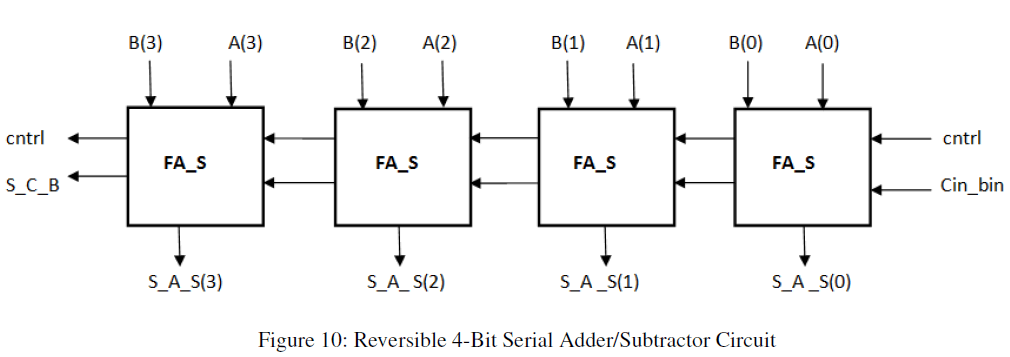
C. Design of reversible 4 bit Serial Adder/Subtractor circuit (SA_S) |
| The designing of this unit can be done with the help of four full adder/ Subtractor circuits. and shown in Fig10.The selection of parallel adder/ subtractor is done by control line. When control signal Ctrl is at logic 0, the circuit acts as serial adder & when Ctrl goes to logic 1, the circuit performs as Serial subtractor |
 |
VII. RESULTS AND DISCUSSIONS |
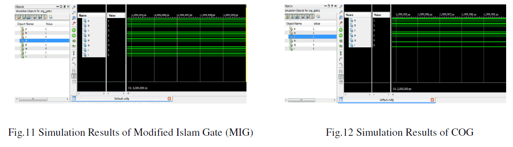
| A.Simulation results for MIG and COG reversible Gates: .The entire architecture is modelled using VHDL. The coding is done on Xilinx ISE8.2i on Spartan 3E using target device: 3s500efg320-4 at speed grade of -4.Simulation can be done using ModelSim SE 6.2h simulator. The simulation result for MIG and COG is shown on Fig. 11 & Fig. 12. |
 |
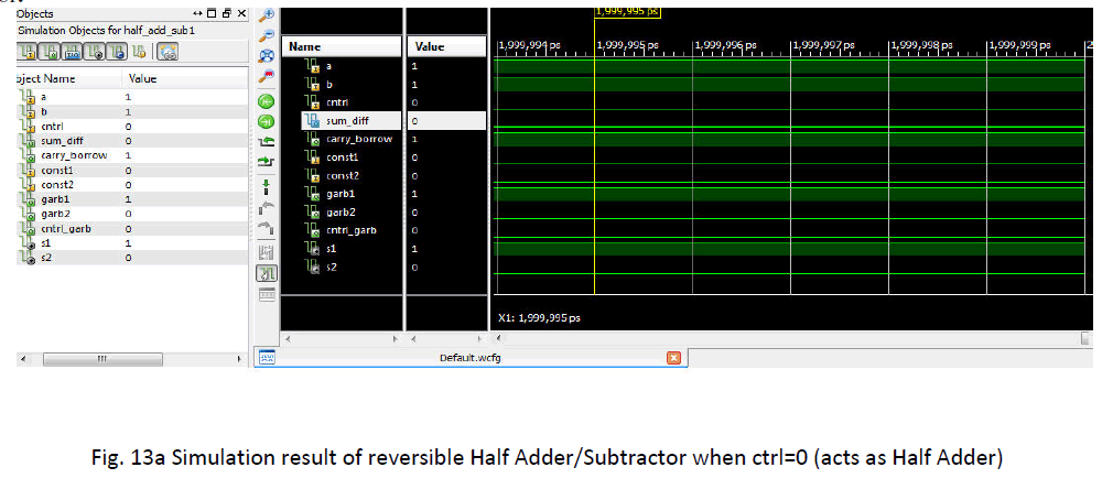
| B.Simulation results for Half Adder/Subtractor: The Simulation results for Half adder/Subtractor is shown below. When the ctrl=0 it acts as Half Adder and the simulation is shown in Fig. 13a. The coding is done on Xilinx ISE8.2i on Spartan 3E using target device: 3s500efg320-4 at speed grade of -4.Simulation can be done using ModelSim SE 6.2h simulator. |
 |
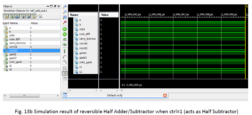
| When the ctrl=1 it acts as Half Subtractor and the simulation is shown in Fig. 13b. The coding is done on Xilinx ISE8.2i on Spartan 3E using target device: 3s500efg320-4 at speed grade of -4.Simulation can be done using ModelSim SE 6.2h simulator |
 |
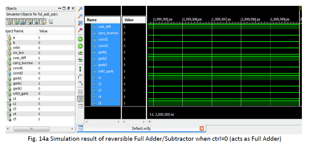
| C. Simulation results for Full Adder/Subtractor: The Simulation results for Half adder/Subtractor is shown below. When the ctrl=0 it acts as Full Adder and the simulation is shown in Fig. 14a. The coding is done on Xilinx ISE8.2i on Spartan 3E using target device: 3s500efg320-4 at speed grade of -4.Simulation can be done using ModelSim SE 6.2h simulator |
 |
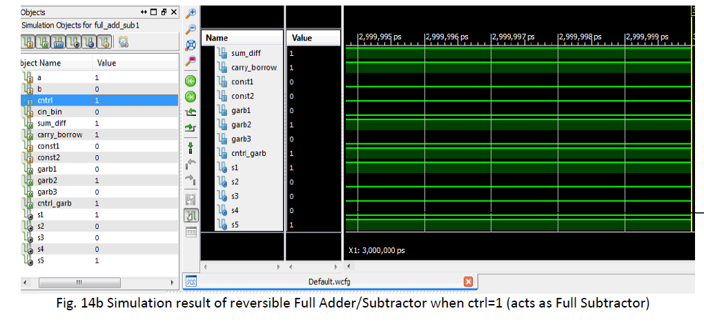
| When the ctrl=1 it acts as Full Subtractor and the simulation is shown in Fig. 14b. The coding is done on Xilinx ISE8.2i on Spartan 3E using target device: 3s500efg320-4 at speed grade of -4.Simulation can be done using ModelSim SE 6.2h simulator |
 |
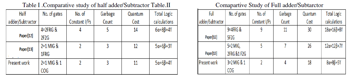
| The Table I and Table II shows the comparative results of different reversible Half Adder/Subtractor, Full Adder/Subtractor. From the tables it is shown that in the present work gate count, Garbage count, quantum cost is minimized. |
 |
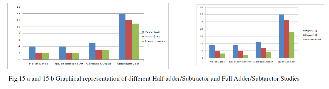
| The Fig 15a and 15b shows the comparative results of different reversible Half Adder/Subtractor, Full Adder/Subtractor in the Graph form. From the graphs it is shown that in the present work gate count, Garbage count, quantum cost is minimized. |
 |
VIII.CONCLUSION |
| This paper presents an efficient design of reversible full adder/subtractor and Serial adder/subtractor. The proposed design can work as a single unit that can act as adder as well as subtractor on the requirement. We have compared these proposed design with the existing designs [12,13] in terms of reversible gates used, Garbage outputs, constant inputs,Quantum cost and Hardware Complexity The proposed work reduces hardware complexity, reduces gate count, reduces garbage bits and constant inputs.. In future we are planning to design more efficient Adder/Subtractor design and other reversible circuits with less garbage bits and constant input. |
ACKNOWLEDGEMENT |
| The author acknowledges to her co-author for their kind support and help during the research. This work is supported by Department of ECE, B.B.S.B.E.C ,Fatehgarh Sahib, Punjab |
References |
|