International Journal of Advanced Research in Electrical, Electronics and Instrumentation Engineering
ISSN ONLINE(2278-8875) PRINT (2320-3765)
ISSN ONLINE(2278-8875) PRINT (2320-3765)
Leeba Varghese 1, Suranya G.2
|
| Related article at Pubmed, Scholar Google |
Visit for more related articles at International Journal of Advanced Research in Electrical, Electronics and Instrumentation Engineering
In this paper we present LFSR reseeding scheme for BIST. A time -to –market efficient algorithm is introduced for selecting reseeding points in the test sequence. This algorithm targets complete fault coverage and minimization of the test length. Functional broadside tests that avoid over testing by ensuring that a circuit traverses only reachable states during the functional clock cycles of a test[1]. These consist of the input vectors and the corresponding responses. They check for proper operation of a verified design by testing the internal chip nodes. Functional tests cover a very high percentage of modeled faults in logic circuits and their generation is the main topic of this paper. Function test sequence are generated by LFSR. Often, functional vectors are understood as verification vectors, which are used to verify whether the hardware actually matches its specification. However, in the ATE world, any vectors applied are understood to be functional fault coverage vectors applied during manufacturing test. This paper shows the on chip test Generation for a bench mark circuit using simple fixed hardware design with small no of parameters altered in the design for the generation of no of patterns. If the patterns of the input test vector results a fault simulation then circuit test is going to fail.
Keywords |
| BIST, LFSR, Functional Test, resseding. |
INTRODUCTION |
| Very Large Scale Integration (VLSI) has made a dramatic impact on the growth of integrated circuit technology. It has not only reduced the size and the cost but also increased the complexity of the circuits. The positive improvements have resulted in significant performance/cost advantages in VLSI systems. There are, however, potential problems which may retard the effective use and growth of future VLSI technology. Among these is the problem of circuit testing, which becomes increasingly difficult as the scale of integration grows. Because of the high device counts and limited input/output access that characterize VLSI circuits, conventional testing approaches are often ineffective and insufficient for VLSI circuits. Built-in self-test (BIST) is a commonly used design technique that allows a circuit to test itself. BIST has gained popularity as an effective solution over circuit test cost, test quality and test reuse problems. In this paper we are presenting an implementation of a tester using Verilog. Test time is a significant component of IC cost. It needs to be minimized and yet has to have maximum coverage to ensure zero-defect. The goal of testing is to apply a minimum set of input vectors to the device to determine if it contains a defect. Costs increase dramatically as faulty components find their way into higher levels of integration. Thus, there is a need for design for testability techniques. |
| For any testing methodology, the following factors should be considered- high and easily verifiable fault coverage, minimum test pattern generation, minimum performance degradation, at-speed testing, short testing time, and reasonable hardware overhead. With increasing integration density, the amount of manufacture faults is increasing Thus, we have to test the chip. With increasing complexity of the design, it becomes impossible to test the chip externally Thus , we have to use BIST Built-In Self-Test (BIST) provides a feasible solution to the above demands. Another advantage of this methodology is that the test patterns are not applied by external Automatic Test Equipments (ATEs) but generated by in built testing circuit. It saves the memory requirement during test. BIST (Built-In Self-Test) : Is a design technique in which parts of a circuit are used to test the circuit itself. |
| Over testing due to the application of two-patterns scan-based tests was described in [2]–[4]. Slow paths that cannot be sensitized during functional operation may cause the circuit to fail [2]. In addition, current demands that are higher than those possible during functional operation may cause voltage drops that will slow the circuit and cause it to fail [3], [4]. In both cases, the circuit will operate correctly during functional operation. |
| Functional broadside tests [5] ensure that the scan-in state is a state that the circuit can enter during functional operation, or a reachable state. As broadside tests [6], they operate the circuit in functional mode for two clock cycles after an initial state is scanned in. This results in the application of a two-pattern test. |
| Delay faults that are detected by the test can also affect functional operation.Test generation procedures for functional and pseudo-functional scan-based tests were described in [5] and [7]–[14]. The procedures generate test sets offline for application from an external tester. |
| This work considers the on-chip (or built-in) generation of functional broadside tests. On-chip test generation reduces the test data volume and facilitates at-speed test application. On-chip test generation methods for delay faults, such as the ones described in [15] . The on-chip test generation method from [15] applies pseudo-functional test generation based on LFSR reseeding scheme . The on-chip test generation process described in this work guarantees that only reachable states will be used.However, the tests that are needed for achieving this higher fault coverage are also ones that can cause over testing. |
| If a primary input sequence A is applied in functional mode starting from a reachable state, all the states traversed under A are reachable states. Any one of these states can be used as the initial state for the application of a functional broadside test. By generating A on-chip and ensuring that it takes the circuit through a varied set of reachable states, the on-chip test generation process is able to achieve high transition fault coverage using functional broadside tests based on A. |
| The hardware used in this paper for generating the primary input sequence A consists of a resseding scheme with linear-feedback shift-register (LFSR) as a random source [15], and of a small number of gates (atmost six gates are needed for every one of the benchmark circuits considered). The gates are used for modifying the random sequence in order to avoid cases where the sequence takes the circuit into the same or similar reachable states repeatedly. This is referred to as repeated synchronization [13]. In addition, the on-chip test generation hardware consists of a single gate that is used for determining which tests based on will be applied to the circuit. The result is a simple and fixed hardware structure, which is tailored to a given circuit only through the following parameters. |
| 1) The number of LFSR bits. |
| 2) The length of the primary input sequence. |
| 3) The specific gates used for modifying the LFSR sequence into the sequence. |
| 4) The specific gate used for selecting the functional broadside tests that will be applied to the circuit based on. |
| 5) Seeds for the LFSR in order to generate several primary input sequences and several subsets of tests. |
BLOCK DIAGRAM OF BIST WITH LFSR RESEEDING SCHEME |
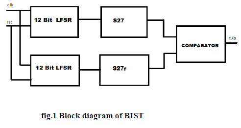 |
| Generate test vectors, apply them to the circuit under test (CUT) or device under test (DUT), and then verify the response.Fig.1 shows a simple BIST block diagram which uses a linear feedback shift register (LFSR)with reseeding scheme to generate the test vectors for circuit under test. LFSR is used as a pseudorandom sequence generator. In this paper we are testing the functional operation of reference circuits .For this we need to check Maximum possible input conditional that may activate the each and every element in the IC. By this we can check each and every transistor in the IC and will know is that IC working perfectly or not.In our project we use 12 bit LFSR for generate 12bit random patterns. By using some basic digital gates we convert these 12bit patterns into 4bit patterns.These patterns are applied to the S27 Benchmark Circuit. This is reference circuits in our project. It need four inputs. For 4bit inputs there are 16 different combinations in digital. But we don’t need those 16 combinations we require 4 patterns to check the complete IC and its functional operation.We generate that particular input patters which are required to check IC. |
A. LFSR RESEEDING SCHEME |
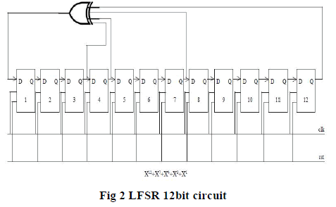
| Linear Feedback Shift Registers (LFSR) can generate good pseudorandom patterns. Clock is the only signal which is required to generate those test patterns.When the LFSR is clocked after giving the input seed to the LFSR, it will generate all the possible test patterns for the input seed for each clock. Note that the seed value can be anything except all 0’s, which produces all the test patterns as 0. The LFSR generates it patterns according to its feedback polynomial. The LFSR has the behaviour of achieving high-fault coverage by reducing correlation among the test patterns. |
1 Algorithmic Test Generation |
| List primary inputs controlling location where a fault should be detected. |
| Determine primary input conditions to activate a fault and to sensitize the primary outputs such that the fault can be observed. |
2 Linear Feedback Shift Registers (LFSRs) |
| Linear feedback shift register (LSFR) is a shift register whose input bit is a linear function of its previous state. The only linear function of single bits is XOR, thus it is a shift register whose input bit is driven by the exclusive-or (XOR) of some bits of the overall shift register value flops. The initial value of the LFSR is called the seed, and the operation of the register is deterministic, the stream of values produced by the register is completely determined by its current (or previous) state. |
| The seed is used to generate a test pattern and their corresponding test cube. Reseeding is a very powerful method for reducingtest data. Most of the test data reduction is mainlyconcentrating on LFSR reseeding. The basic idea inLFSR reseeding is to generate deterministic test cubes by expanding seeds. A seed is an initial state of the LFSR that is expanded by running the LFSR in autonomous mode. |
| An LFSR generates periodic sequence must start in a non-zero state, The maximum length of an LFSR sequence is 2n -1 does not generate all 0s pattern. |
 |
RESEEDING SCHEME |
| To focus on reducing test pattern with effective Linear Feedback Shift Register (LFSR) reseeding. LFSR is a good pseudorandom pattern generator which generates all possible test vectors with the help of the tap sequence. It can achieve high fault coverage by reducing correlation between the test vectors. Reseeding is a powerful method for reducing the test data volume and storage. This study presents a new LFSR reseeding technique for efficient reduction of test pattern. A new encoding technique is proposed in this study which is used to reduce the size of the test data. Size of the test data can be reduced by LFSR clock which is inactive for several clock cycles after the input seed is given. When the clock goes to inactive state, a rotate right shift operation is done on the seed to get all the remaining possible values. After getting all the possible values for that seed a new seed is given by making the clock active. Test data volume is reduced by storing the data only when the clock is active. With in the reduced clocks, rest of all the remaining test vectors was derived. A special Control logic is used to make the clock active as well as inactive. HERE SEED IS 101001 100100 |
B. GENERATION OF PRIMARY INPUT SEQUENCE |
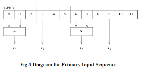 |
| The 12-bit LFSR is shown at the top of Fig. Bits0, 1 and 2 of the LFSR are used for producing the values of I0. The OR gate is driven by bits 0 and 1 of the LFSR. Bit 2 of the LFSR reduces the dependencies between the values of I0 and the values of I1. Bits 3, 4, and 5 of the LFSR are used for producing the values of I1 . Therefore,I1 is driven directly by bit 3of the LFSR. Bits 4 and 5 reduce the dependencies between the values of I1 and the values of I2.Bits 6, 7, and 8 are used for producing the values of I2. The AND gate is driven by bits 6 and 7. Bit 8 of the LFSR reduces the dependencies between the values of I2and I3.Finally, bits 9, 10, and 11 are used for producing the valuesof I3. Therefore, I3 is driven directly by bit 9 of the LFSR. |
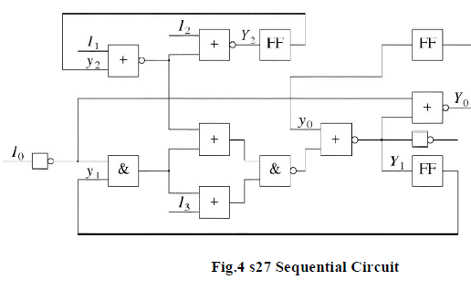
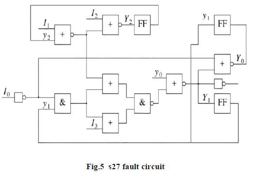
C. SEQUENTIAL BENCHMARK CIRCUIT s27 |
| Logic Gates are taken at Primary input combination in (2^4=16). S27 circuit have three scan circuits (f/f „s) and then its scan inputs are 2^3=8. Scan-in-state input are s0, s1, s2 and it’s scanned out denoted as s. S27 bench mark circuit is the standard sequential circuit. Here we are used s27 bench mark circuit for as a testing circuit.Applying test vectors as input to the s27 bench mark sequential circuit.I0, I1, I2, I3 are the input of this circuit. |
 |
 |
D. COMPARATOR |
| The comparator will produce a logic 1 in the case of any mismatch between the expectedand actual output responses. comparator to detect mismatches in the fault-free and faulty circuits.Comparator is used to compare the two output coming from fault circuit and fault free circuit.Both output are same :zero,otherwise 1. |
RESULT ANALYIS |
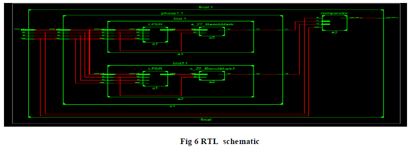
A. RTL SCHEMATIC |
| Here test vectors given to the input of cut and detect the fault from fault free circuit and faulty circuit by using comparator. Corresponding output waveform are given below. |
 |
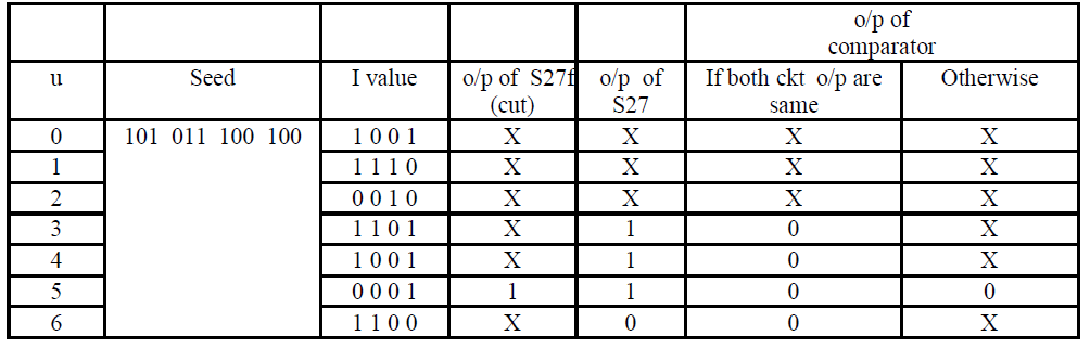
B.Truth table |
 |
 |
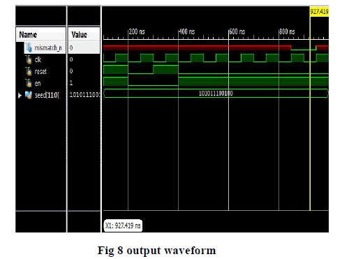
C. Output waveform |
| Here we can see the seed of the LFSR ,and enable signal, reset ,clock signal,mismatch values.the output of comparator is mismatch _n.from this graph we can conclude the cut is not matches with the fault free circuit. |
 |
CONCLUSION |
| The presence of delay-inducing defects is causing increasing concern in the semiconductor industry today. To test for such delay-inducing defects, onchip testing techniques are being implemented. On-chip test generation has the advantage It reduces test data volume, Facilitates at-speed test application, Achieves high fault coverage.The hardware used in this paper for generating the primary input sequence A consists of a linear-feedback shift-register (LFSR) as a random source and of a small number of gates. To focus on reducing test pattern with effective Linear Feedback Shift Register (LFSR) reseeding. |
References |
|