International Journal of Advanced Research in Electrical, Electronics and Instrumentation Engineering
ISSN ONLINE(2278-8875) PRINT (2320-3765)
ISSN ONLINE(2278-8875) PRINT (2320-3765)
GaneshBabu.J 1, Radhika.P2
|
| Related article at Pubmed, Scholar Google |
Visit for more related articles at International Journal of Advanced Research in Electrical, Electronics and Instrumentation Engineering
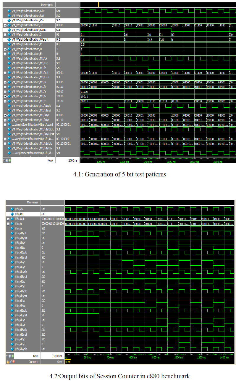
Pseudorandom built-in self test (BIST) generators have been widely utilized to test integrated circuit and systems. In this Project an accumulator-based-3 weight test pattern generation scheme is presented and proposed scheme generates set of test patterns with weights 0, 0.5 and 1. These accumulators are mostly found in current VLSI chips and that the scheme can be efficiently to drive the hardware of BIST pattern generation. The hardware requirements for this project are FPGA SPARTAN 3 and the software which are used as Modelsim and Xilinx . Finally test patterns are produced for 5bit and c880 testbench circuits.
Keywords |
| Three weights 0-0.5-1, Accumulator, c880, D flipflop. |
INTRODUCTION |
| BIST is a design-for-testability technique that places the testing functions physically with the circuit under test (CUT). The basic BIST architecture requires the addition of three hardware blocks to a digital circuit: a test pattern generator, a response analyzer, and a test controller. The test pattern generator generates the test patterns for the CUT. Examples of pattern generators are a ROM with stored patterns, a counter, and a linear feedback shift register (LFSR). A typical response analyzer is a comparator with stored responses or an LFSR used as a signature analyzer. It compacts and analyzes the test responses to determine correctness of the CUT. A test control block is necessary to activate the test and analyze the responses. However, in general, several test-related functions can be executed through a test controller circuit.A digital system is tested and diagnosed during its lifetime on numerous occasions. Such a test and diagnosis should be quick and have very high fault coverage. One way to ensure this is to specify such a testing to as one of the system functions, so now it is called Built In Self Test (BIST). With properly designed BIST, the cost of added test hardware will be more than balanced by the benefits in terms of reliability and reduced maintenance cost. For BIST, we would require that the test patterns be generated on the system/chip itself. However, this should be done keeping in mind that the additional hardware is minimized. One extreme is to use exhaustive testing using a counter and storing the results for each fault simulation at a place on the chip (like ROM). An n input circuit would then require 2^n combinations which can be very tiresome on the system with respect to the space and the time. Also, more the number of transitions, the power consumed will be more. |
TEST PATTERN GENERATION THROUGH ACCUMULATOR BASED 3 WEIGHT. |
| A new weighted random pattern design for testability is described where the shift register latches distributed throughout the chip are modified so that they can generate biased pseudo-random patterns upon demand. A two-bit code is transmitted to each weighted random pattern shift register latches to determine its specific weight. The weighted random pattern test is then divided into groups, where each group is activated with a different set of weights. The weights are dynamically adjusted during the course of the test to "go after" the remaining untested faults.An accumulator-based 3-weight test pattern generation scheme is presented; the proposed scheme generates set of patterns with weights 0, 0.5, and 1. Since accumulators are commonly found in current VLSI chips, this scheme can be efficiently utilized to drive down the hardware of built in self test pattern generation, as well. Comparisons with previously presented schemes indicate that the proposed scheme compares favorably with respect to the required hardware. |
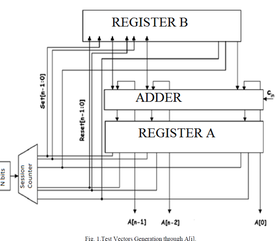 |
OPERATION OF THE CELL: |
| I. For A[i] =1 , We give set[i]=1 and reset[i]=0 and hence A[i]=1 and B[i]=0. Then the output is equal to 1,and Cin will be equal to Co. Cin is transferred to the Cout. |
| II. For A[i] =0 , We give set[i]=0 and reset[i]=1 and hence A[i]=0 and B[i]=1. Then the output is equal to 0, and here Cin is equal to Cout. Cin is transferred to the Cout. |
| III. For A[i] = “-” , set[i] =0 and reset[i] =0. The D input of the flip-flop of register B is driven by either 1 or 0, depending on the value that will be added to the accumulator inputs in order to generate satisfactorily random patterns to the inputs of the CUT. |
TEST PATTERNS FOR BENCH MARK C880 CIRCUITS |
C880 BENCH MARK CIRCUIT: |
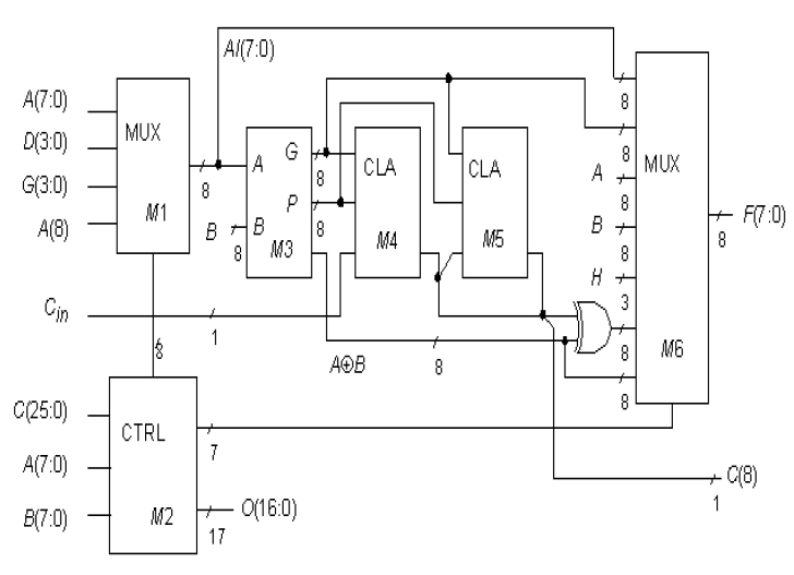
| According to this paper, our future work is to check the performance of the bench mark circuit c880. The Bench mark circuit consists of 60 inputs, 26 outputs, and 383 gates. It’s an 8-bit ALU with high level model. The core of this 8-bit ALU is an 8-bit 74283-style adder. To analyse the C880 we have to modify our proposed test pattern architecture. Because C880 consist of 60 inputs but our proposed testing hardware provides of demo test pattern only. |
 |
PROPOSED SYSTEM ADVANTAGES: |
| It does not impose any requirements about the design of the adder |
| It does not require any modification of the adder. |
| Does not affect the operating speed of the adder. |
PROPOSED SYSTEM APPLICATION: |
| Test to Integrated Circuits and Systems |
| BIST Applications |
SIMULATION RESULTS |
| ModelSim is a simulation tool for hardware design which provides behavioural simulation of a number of languages, i.e., Verilog, VHDL, and System C. Verilog HDL is an industry standard language used to create analog, digital, and mixed-signal circuits. HDL’s are languages which are used to describe the functionality of a piece of hardware as opposed to the execution of sequential instructions like that in a regular software application. |
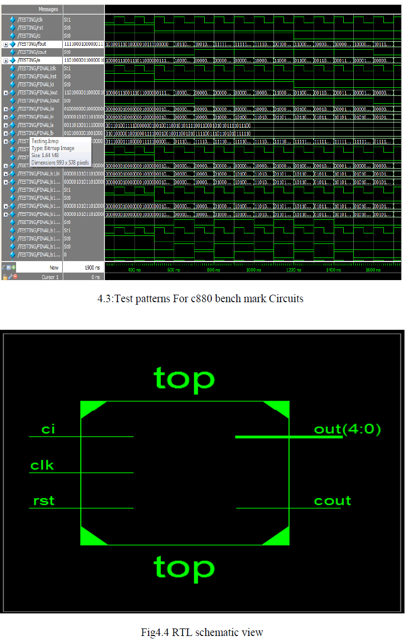
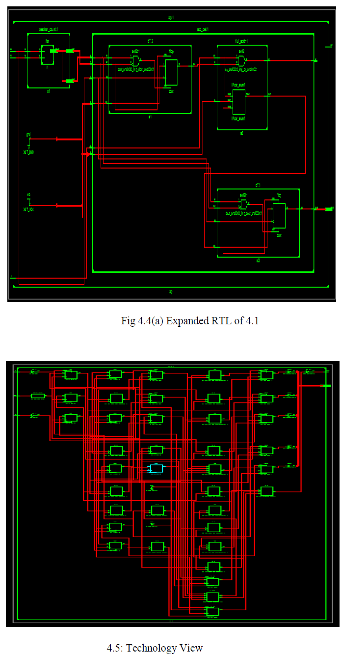
| Verilog code is generated for this accumulator circuit using 6.4c.Then RTL schematic is produced using XILINK 13.2. These test patterns are implemented in FPGA SPARTAN 3(XC3S400 PQ 208). |
 |
 |
 |
CONCLUSION |
| We have presented an accumulator-based 3-weight (0, 0.5, and 1) test-per-clock generation scheme, which can be utilized to efficiently generate weighted patterns without altering the structure of the adder. It does not impose any requirements about the design of the adder and operating speed is not affected. Benchmark net-lists demonstrate that the fault coverage of the proposed pattern generator is significantly higher compared to conventional pattern generation techniques. |
References |
|