International Journal of Advanced Research in Electrical, Electronics and Instrumentation Engineering
ISSN ONLINE(2278-8875) PRINT (2320-3765)
ISSN ONLINE(2278-8875) PRINT (2320-3765)
Sabir Hussain1 K Padma Priya2
|
| Related article at Pubmed, Scholar Google |
Visit for more related articles at International Journal of Advanced Research in Electrical, Electronics and Instrumentation Engineering
This research article proposed a logic BIST using linear feedback shift register (LFSR) to generate low power test patterns; It reduced the number of transitions at the input of the circuit-under-test using bit swapping technique. The designed architecture is programmed using Verilog HDL and simulated using CADENCE EDA Tool of 180 nm technology and also proposed design gives better performance in term of power dissipation as compared to standard LFSR.
Keywords |
| Low power, Test Pattern Generation, Linear Feedback Shift Register, Logic Built in Self Test |
INTRODUCTION |
| The main challenging areas in VLSI are performance, cost, power dissipation is due to switching i.e. the power consumed testing, due to short circuit current flow and charging of load area, reliability and power. The demand for portable computing devices and communications system are increasing rapidly. The applications require low power dissipation VLSI circuits. The power dissipation during test mode is 200% more than in normal mode. Hence the important aspect to optimize power during testing [1]. |
| Power dissipation is a challenging problem for today’s System-on-Chips (SoCs) design and test. The power dissipation in CMOS technology is either static or dynamic. Static power dissipation is primarily due to the leakage currents and contribution to the total power dissipation is very small. The dominant factor in the power dissipation is the dynamic power which is consumed when the circuit nodes switch from 0 to 1. During switching, the power is consumed due to the short circuit current flow and the charging of load capacitances is given by equation. |
| Pavg = αT.Cload.Vdd.fclk |
| Where; αT is the switching activity factor of the gate. Cload is represents the total load capacitance. |
| Vdd is the supply voltage fclk represents the operating frequency. |
| The average power is directly proportional to the αT. The power dissipation during testing can be reduced by controlling the switching activity and the load capacitance here dynamic power dissipation contributed to total power dissipation .The above equation dynamic power depends on three parameters: supply voltage, clock frequency and switching activity. To reduce the dynamic power dissipation by using first two parameters only at the expense of circuit performance. But power reduction using the switching activity doesn't degrade the performance of the circuit. Power dissipation during testing is one of most important issue [2] |
| Latest advances in semiconductor technology have led to transistor scaling of transistor dimensions, allowing a large number of devices to be fabricated on a single chip. The high integration has made power consumption. In addition the ever increasing utilization of portable computing devices and communication systems requires low power dissipation in VLSI circuits [3]. |
| The power dissipation of a system in test mode is more than in normal mode. Low correlation between consecutive test vectors (e.g. among pseudorandom patterns) increases switching activity and eventually power dissipation in the circuit. The same happens when applying low correlated patterns to scan chains. Increasing switching activity in scanchain results in increasing power consumption in scan chain and combinational block. The extra power (average or peak) can cause problems such as instantaneous power surge causes circuit damage, formation of hot spots difficulty in performance verification and reduction of the product yield and lifetime [4]. |
PRIOR WORK |
| Intensive research efforts have been devoted to develop techniques and algorithms to reduce average power consumption at different levels of abstraction. |
| System-Level Partitioning and Scheduling this technique proposed in [5] consists of a distributed BIST control scheme that simplifies BIST architecture for complex ICs, especially during higher levels of test activity. This approach can schedule the execution of every BIST element to keep the power dissipation under a specified limit. The proposed approach [6] targets the average power consumption during normal circuit operations; they do not concern the average power consumption during test. The method proposed in [7] use random single input change (RISC) test generation, which is used to generate low power test pattern. In this method, power consumption is reduced but at the additional cost is between 19% and 13%.Another technique was proposed in [8] this approach proposed a low transition LFSR for BIST applications. This reduces the average and peak power of circuit during testing. In [9] approach fault model and ATPG algorithm is chosen first and then test pattern are generated to obtain the desire fault coverage. |
| In this paper we propose low power BIST architecture, inspired by the precomputation architecture [10], and particularly suited when pseudo-random test generation is adopted. Since each vector applied to the Circuit under test (CUT) consumes power, the rationale behind our architecture is to apply to CUT the minimum number of test vectors required to attain the desired Fault Coverage (FC). We propose an algorithm to filter the test vectors coming from a given Test Pattern Generator (TPG) consist of low power test patterns that reduces the number of transitions at the input of the circuit-under-test using bit swapping technique and to synthesize is done to extract power . This architecture effectively reduces the switching activity at the circuit inputs, reducing the average power consumption during test application. Experimental results performed on the Logical adder circuit show a reduction in the average power consumption during test is 25.11% with a negligible hardware overhead. The remainder of the paper is organized as follows: Sections III and IV describe the BIST Architecture and standard LFSR and section V and VI describe our low power LFSR and its properties, while remaining section reports some experimental results. Finally, Section VIII draws some conclusions. |
ARCHITECTURE |
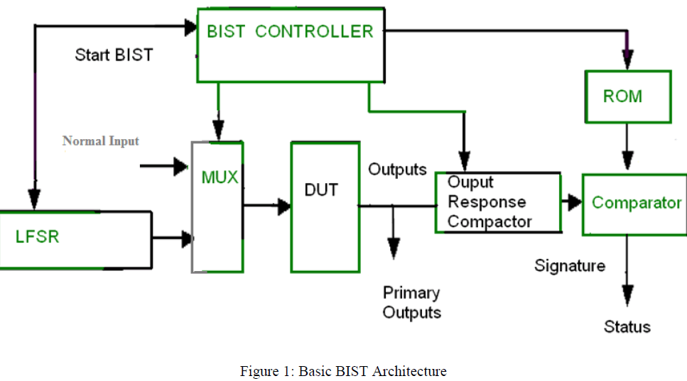
| BIST is basically same as off-line testing using ATE where the test pattern generator and the test response analyzer are on-chip circuitry (instead of equipments). As equipments are replaced by circuitry, so it is obvious that compressed implementations of test pattern generator and response analyzer are to be designed [11]. The basic architecture of BIST is shown in Figure 1 |
| Hardware Test Pattern Generator: This module generates the test patterns required to sensitize the faults and propagate the effect to the outputs (of the CUT). As the test pattern generator is a circuit (not equipment) its area is limited. So storing and then generating test patterns obtained by ATPG [1-3] algorithms on the CUT using the hardware test pattern generator is not feasible. In other words, the test pattern generator cannot be a memory where all test patters obtained by running ATPG algorithms (or random pattern generation algorithms) on the CUT are stored and applied during execution of the BIST [2]. Instead, the test pattern generator is basically a type of register which generates random patterns which act as test patterns. The main emphasis of the register design is to have low area yet generate as many different patterns (from 0 to 2n, if there are n flip-flops in the register) as possible. Input Multiplexer: This multiplexer is to allow normal inputs to the circuit when it is operational and test inputs from the pattern generator when BIST is executed. The control input of the multiplexer is fed by a central test controller. Output response compactor: Output response compacter performs lossy compression of the outputs of the CUT (here we have used Half adder to test). As in the case of off-line testing, in BIST the output of the CUT is to be compared with the expected response (called golden signature). If CUT output does not match the expected response, fault is detected. Similar to the situation for test pattern generator, expected output responses cannot be stored explicitly in a memory and compared with the responses of the CUT. |
| Read Only Memory (ROM): Stores golden signature that needs to be compared with the compacted CUT response. |
| Comparator: Hardware to compare compacted CUT response and golden signature (from ROM). |
| Test Controller: Circuit to control the BIST. Whenever an IC is powered up (signal start BIST is made active) the test controller starts the BIST procedure. Once the test is over, the status line is made high if fault is found. Following that, the controller connects normal inputs to the CUT via the multiplexer, thus making it ready for operation. Among the modules discussed above, the most important one is hardware test pattern generator (LFSR).The other ones are standard digital blocks. In the next two sections we will discuss this blocks in details. |
 |
PROPOSED LOW POWER LFSR |
| The proposed low power LFSR technique uses bit swapping technique to reduce the peak power. By connecting multiplexers on the LFSR register. the number of transitions are decreased for that cell which are under bit swapping. The number of transitions in each register in LFSR without applying bit swapping technique here two cells in an nbit LFSR [3] are considered to be adjacent if the output of one cell feeds the input of the second directly (i.e., without an intervening XOR gate). Each cell in a maximal-length n-stage LFSR (internal or external) will produce a number of transitions equal to 2n-1 after going through a sequence of 2n clock cycles. The sequence of 1s and 0s that is followed by one bit position of a maximal-length LFSR is commonly referred to as an m sequence. Each bit within the LFSR will follow the same m sequence with a one-time-step delay. The m-sequence generated by an LFSR of length n has a periodicity of 2n-1. It is a well-known standard property of an m-sequence of length n that the total number of runs of consecutive occurrences of the same binary digit is 2n-1.The beginning of each run is marked by a transition between 0 and 1.Therefore, the total number of transitions for each stage of the LFSR is 2n-1. |
| The Function of LFSR Explains here c1 in the next state is determined by “c1 xor with cn” in the present state. It is important to note that the overall savings of 25% is not equally distributed between the outputs of the multiplexers. This is because the value of c1 in the present state will affect the value of c2 and its own value in the next state (c2 (Next) = c1 andc1 (Next) = “c1 xor cn”). Dividing one figure by the other, we see that the total number of transitions saved at O2 is 50%. |
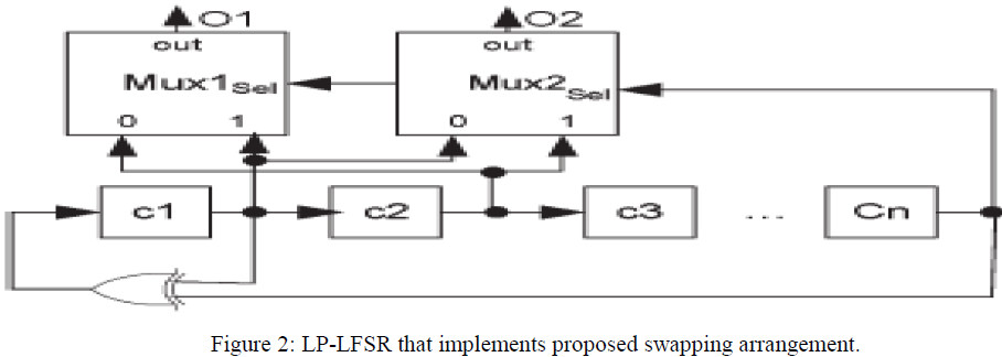
| In this type, the LFSR structure is modified to apply swapping between the neighbouring bits. The last bit is the selection line for the swapping process; if the last bit is 0, then swapping is performed, otherwise, nothing will change. It was proved that the BS-LFSR reduces the switching activity in the inputs of the Circuit Under Testing about 25%. Figure 2 illustrates this type of LFSR [12] |
 |
PROPERTIES OF THE LOW POWER LFSR |
| There are some important features of the LP-LFSR that make it equivalent to a conventional LFSR. The most important properties of the BS-LFSR are the following. |
| The LP-LFSR generates the same number of 1s and 0s at the output of multiplexers after swapping of two adjacent cells[8]. hence, the probabilities of having a 0 or 1 at a certain cell of the scan chain before applying the test vectors are equal. Hence the proposed design retains an important feature of any random TPG. Furthermore, the output of the multiplexer depends on three different cells of the LFSR, each of which contains a pseudorandom value. Hence, the expected value at the output can also be considered to be a pseudorandom value. |
| If the LP-LFSR is used to generate test patterns for either test per- clock BIST or for the primary inputs of a scanbased sequential circuit (assuming that they are directly accessible) as shown in Fig. 3, then consider the case that c1 will be swapped with c2 and c3 with c4, . . . , cn-2 with cn-1 according to the value of cn which is connected to the selection line of the multiplexers. In this case, we have the same exhaustive set of test vectors as would be generated by the conventional LFSR, but their order will be different and the overall transitions in the primary inputs of the CUT will be reduced by 26%.The different transition values of LFSR and LPLFSR. |
EXPERIMENTAL RESULTS |
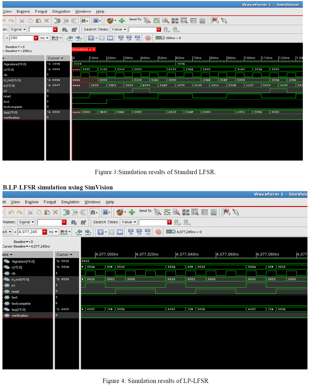
| To validate the effectiveness of the proposed approach we select traditional LFSR technique for comparison, simulation and synthesis were carried out with Cadence SimVision and Cadence RTL Compiler GPDK 180nm CMOS library is used. |
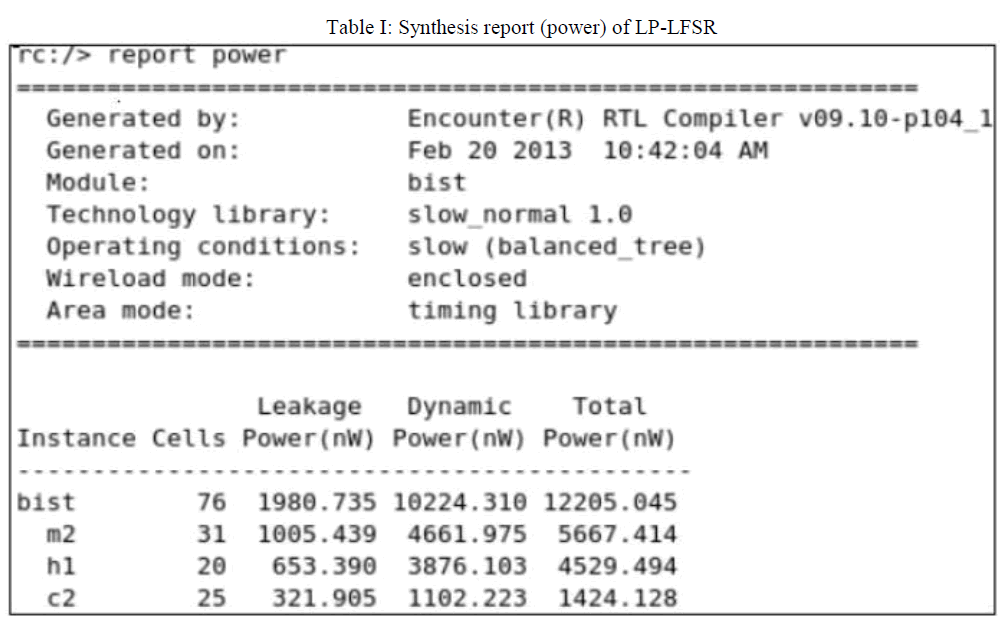
| In our experimentation we used the polynomial for both LFSR and LP-LFSR. The test patterns are generated using an LFSR written in verilog HDL program. As we used 16-bit Logical Adder as Circuit under test. Figure 3 and 4 shows the simulation result of Standard LFSR and LP-LFSR respectively and Figure 5 and 6 shows RTL schematic and power report extracted from Cadence RTL compiler. |
A.Standard LFSR simulation using SimVision |
 |
C.Power Calculation Using Cadence RTL Compiler |
 |
POWER CONSUMPTION COMPARISON |
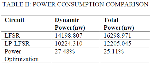
| The Table II shows the comparison of experimental results of the test power consumption with the proposed method. In Table I the columns refers to the test power consumption with Standard LFSR circuit. It can be found that the LFSR circuit consumes 16.29 mw (16298.971nw) test power where as the LP-LFSR circuit consumes12.20mw (12205.045nw) test power with 26% improvement of power consumption during testing. |
 |
CONCLUSION |
| This paper presented a Low Power LFSR architecture for Logic Built In Self Test. This is general and can be applied to almost all Test Pattern Generators. Our method is based on swapping the adjacent bit pairs depending on the status of the last bit value. Swapping is performed if the last bit of Pseudo Random Pattern is 0 and it is left unchanged if the last bit is 0. A considerable amount i.e. 27.48% of dynamic power saving was achieved with the help of this technique. After adding it with static (or leakage) power, we got the net power and the net power saving was 25.11%. |
References |
|