International Journal of Advanced Research in Electrical, Electronics and Instrumentation Engineering
ISSN ONLINE(2278-8875) PRINT (2320-3765)
ISSN ONLINE(2278-8875) PRINT (2320-3765)
S.Nagaraju1, Ch.N.L.Sujatha2, J.S.S.Ramaraju3
|
| Related article at Pubmed, Scholar Google |
Visit for more related articles at International Journal of Advanced Research in Electrical, Electronics and Instrumentation Engineering
In the proposed method we are test the S27 sequential circuit by using Built in Self Test.This paper describes an on-chip test generation method for functional broadside tests. The hardware was base on the application of primary input sequences initial from a well-known reachable state, therefore using the circuit to produce additional reachable states. Random primary enter sequences were changed to avoid repeated synchronization and thus defer varied sets of reachable states. Functional broadside tests are two-pattern scan based tests that avoid over testing by ensuring that a circuit traverses only reachable states in the functional clock cycles of a check. These consist of the input vectors and the equivalent responses. They check for proper operation of a verified design by testing the internal chip nodes. Useful tests cover a very high percentage of modeled faults in logic circuits and their generation is the main topic of this method. Often, functional vectors are understood as verification vectors, these are used to verify whether the hardware actually matches its specification. Though, in the ATE world, any one vectors applied are understood to be functional fault coverage vectors applied during developing test. This paper show the on chip test Generation for a bench mark circuit using simple fixed hardware design with small no of parameters altered in the design for the generation of no of patterns. If the patterns of the input test vector results a fault simulation then circuit test is going to fail.
INTRODUCTION |
| Over testing due to the application of two-patterns can-based tests was described in [1]–[3]. Over testing is related to the detection of delay faults under non-functional operation situation. One of the reasons for these non-functional operation conditions is the following. When an arbitrary state is used as a scan-in state, a two-pattern test can take the circuit through state-transitions that cannot occur during functional operation. As a result, slow paths that cannot be sensitized during functional operation may cause the circuit to fail [1]. In addition, current demands that are higher than those possible during functional operation may cause voltage drops that will slow the circuit and cause it to fail [2], [3]. In both cases, the circuit will operate correctly during functional operation. |
| Functional broadside tests [4] ensure that the scan-in state is a state that the circuit can enter during functional operation, or a reachable state. As broadside tests [5], they operate the circuit in functional mode for two clock cycles after an initial state is scanned in. This results in the application of a two-pattern test. |
| Since the scan-in state is a reachable state, the two-pattern test takes the circuit through state-transitions that are guaranteed to be possible during functional operation. Delay faults that are detected by the test can also affect functional operation, and the current demands do not exceed those possible during functional operation. This alleviates the type of over testing described in [1]–[3]. In addition, the power dissipation during fast functional clock cycles of functional broadside tests does not exceed that possible during functional operation. |
| Test generation procedures for functional and pseudo-functional scan-based tests were described in [4] and [6]–[13]. The procedures generate test sets offline for application from an external tester. Functional scan-based tests use only reachable states as scan-in states. Pseudo-functional scan-based tests use functional constraints to avoid unreachable states that are captured by the constraints. |
| This work considers the on-chip (or built-in) generation of functional broadside tests. On-chip test generation reduces the test data volume and facilitates at-speed test application. On-chip test generation methods for delay faults, such as the ones described in [14] and [15], do not impose any constraints on the states used as scan-in states. Experimental results indicate that an arbitrary state used as a scan-in state is unlikely to be a reachable state [4]. The on-chip test generation method from [16] applies pseudo-functional scan-based tests. Such tests are not sufficient for avoiding unreachable states as scan-in states. The on-chip test generation process described in this work guarantees that only reachable states will be used. It should be noted that the delay fault coverage achievable using functional broadside tests is, in general, lower than that achievable using arbitrary broadside tests as in [14], [15] or pseudo-functional broadside tests as in [16]. This is due to the fact that functional broadside tests avoid unreachable scan-instates, which are allowed by the methods described in [14]– [16]. However, the tests that are needed for achieving this higher fault coverage are also ones that can cause over testing. They can also dissipate more power than possible during functional operation. |
| Only functional broadside tests are considered in this work. Under the proposed on-chip test generation method, the circuit is used for generating reachable states during test application. |
| This alleviates the need to compute reachable states or functional constraints by an offline process as in [4], [6]–[13] and [16]. The underlying observation is related to one of the methods used in [4] for offline test generation, and is the following. |
| If a primary input sequence A is applied in functional mode starting from a reachable state, all the states traversed under A are reachable states. Any one of these states can be used as the initial state for the application of a functional broadside test. By generating A on-chip and ensuring that it takes the circuit through a varied set of reachable states, the on-chip test generation process is able to achieve high transition fault coverage using functional broadside tests based on A. It should be noted that, for the detection of a set of faults F, at most |F| different reachable states are required. This number is typically only a small fraction of the number of all the reachable states of the circuit. Thus, the primary input sequence A does not need to take the circuit through all its reachable states, but only through a sufficiently large number relative to |F|, in order to be effective for the detection of target faults. |
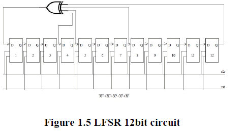
| The hardware used in this paper for generating the primary input sequence A consists of a linear-feedback shift-register (LFSR) as a random source [17], and of a small number of gates (almost six gates are needed for every one of the benchmark circuits considered). The gates are used for modifying the random sequence in order to avoid cases where the sequence takes the circuit into the same or similar reachable states repeatedly. This is referred to as repeated synchronization [18]. In addition, the on-chip test generation hardware consists of a single gate that is used for determining which tests based on will be applied to the circuit. The result is a simple and fixed hardware structure, which is tailored to a given circuit only through the following parameters. |
| 1) The number of LFSR bits. |
| 2) The length of the primary input sequence. |
| 3) The specific gates used for modifying the LFSR sequence into the sequence. |
| 4) The specific gate used for selecting the functional broadside tests that will be applied to the circuit based on. |
| 5) Seeds for the LFSR in order to generate several primary input sequences and several subsets of tests. |
| The on-chip test generation hardware is based on the one described in [19]. It differs from it in the following ways. |
BLOCK DIAGRAM OF LFSR RESEEDING SCHEME |
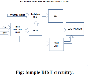 |
| Linear feedback shift register (LSFR) is a shift register whose input bit is a linear function of its previous state. The only linear function of single bits is XOR, thus it is a shift register whose input bit is driven by the exclusive-or (XOR) of some bits of the overall shift register value flops. The initial value of the LFSR is called the seed, and the operation of the register is deterministic, the stream of values produced by the register is completely determined by its current (or previous) state. The seed is used to generate a test pattern and their corresponding test cube. The LFSR length, r, is at least smax+20 where smax is the maximum number of specified bits in any test cube. The r-bit LFSR is initialized with a starting r-bit seed. This initial seed is used to generate the first test cube by running the LFSR for m clock cycles (where m is the scan length) to fill the scan chains. |
BROADSIDE TESTS IN PARTIAL-SCAN CIRCUITS |
| In a full-scan circuit, a broadside test starts by scanning in a state denoted by two primary input vectors, denoted by and are then applied in functional mode. The final state reached at the end of the test is scanned out. The test can be partitioned into two patterns, applied in one functional clock cycle, and applied in a second functional clock cycle. The application of is done under a slow clock to allow signal transitions in the circuit to settle. The application of is done under a fast clock in order to capture delayed signal-transitions. Faults are detected by observing the primary output vector obtained in response to and when the final state is scanned out. In a full scan circuit, the scan-in state is a fully-specified state. After scanning in all the state variables of the circuit are assigned known values. In addition, the values of all the state variables are observed during the scan-out operation at the end of the test. For illustration, we consider a circuit with two primary inputs and five state variables, which are denoted by suppose that and are scanned, an and are un scanned. A possible scan-in state is 000xx, where x stands for an unspecified (unknown) value. In a broadside test for this circuit, may be a partially-specified state as well. For example, suppose that with and we obtain 1x01x. Let we obtain the two-pattern test000xx 00, 1x01x 11. With partially- specified patterns, it may not be possible to activate certain faults. In addition, faults whose effects are propagated by the second pattern to or will not be detected by the scan-out operation at the end of the test. Therefore, it is necessary to consider broadside tests with more than two primary input vectors. The primary input vectors are then applied in functional mode. The state at time unit of the test, where is the next-state obtained when the present-state is and the primary input vector is There is one time unit where such that is applied under a fast clock in order to capture delayed signal-transitions. Application of for such that is done under a slow clock to allow signal-transitions in the circuit to settle. Under the slow clock the circuit operates as a fault free circuit. |
PESUDO RANDOM TEST GENERATION |
| The three primary goals were: |
| (a) to develop a battery of statistical tests to detect non randomness in binary sequences constructed using random number generators and pseudorandom number generators utilized in cryptographic applications, |
| (b) To produce documentation and a software implementation of these tests, and |
| (c) To provide guidance in the use and application of these tests. Pseudorandom- generate patterns that appear to be random but are in fact deterministic (repeatable).Linear Feedback Shift Register (LFSR) Weighted pseudo-random test generation Adaptive pseudo-random test generation |
2.3.1 Algorithmic Test Generation |
| List primary inputs controlling location where a fault should be detected. |
| Determine primary input conditions to activate a fault and to sensitize the primary outputs such that the fault can be observed. |
2.3.2 Linear Feedback Shift Registers (LFSRs) |
| Efficient design for Test Pattern Generators & Output Response Analyzers (also used in CRC) FFs plus a few XOR gates better than counter |
| Fewer gates |
| Higher clock frequency |
| Two types of LFSRs External Feedback, Internal Feedback |
| Higher clock frequency |
| An LFSR generates periodic sequence must start in a non-zero state, The maximum length of an LFSR sequence is 2n -1 does not generate all 0s pattern (gets stuck in that state)The characteristic polynomial of an LFSR generating maximumlength sequence is a primitive polynomial A maximum-length sequence is pseudo-random: number of 1s =number of 0s + 1 same number of runs of consecutive 0s and 1s 1/2 of the runs have length1 1/4 of the runs have length 2 (as long as fractions result in integral numbers of runs). |
 |
 |
 |
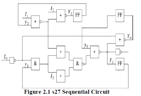
SEQUENTIAL BENCHMARK CIRCUIT s27 |
| Logic Gates are taken at Primary input combination in (2^4=16). |
| S27 circuit have three scan circuits (f/f „s) and then its scan inputs are 2^3=8. |
| S_a_0 fault generates at logic gate (a3). |
| Scan-in-state input are s0, s1, s2 and it’s scanned out denoted as s. |
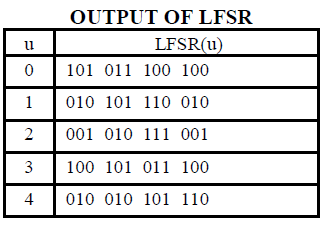
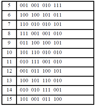
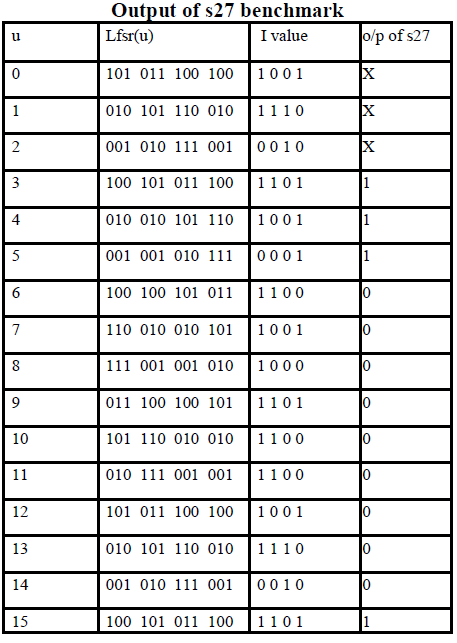
| LFSR register values initially at “1010”. Circuit considered above, let 000xx 00, 1x01x01,0x1xx 01, 11x00 00, 10111 10. We note that is unspecified in the two un scanned state variables. This implies that can be used as a scan-in state instead of and the first two patterns of the test can be omitted. The resulting test would be 0x1x 01.In the scan-in state of this test, we can specify the value of arbitrarily. Suppose that is specified to 1, and suppose that this causes the value of in to be specified to 0.We obtain 011xx 01, 11000 00, 10111 10. The last three states traversed under are 0x1xx, 11x00 and 10111. With more specified values under, more faults are likely to be detected. In general, to obtain a shorter test from a given test of length, we consider we search for the highest time unit such that has unspecified values on all the un scanned since is selected such that it is unspecified on the un scanned state variables. For a full-scan circuit, all the tests will be of length two. This is due to the fact that all the states are fully-specified. |
 |
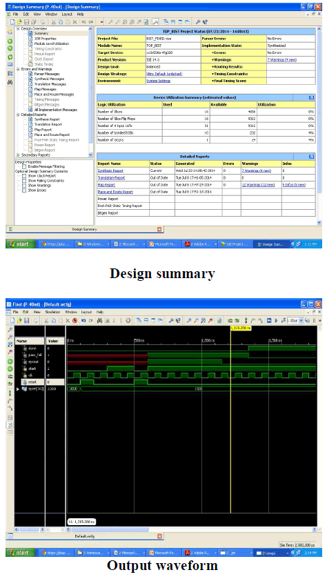
| S27 bench mark circuit is the standard sequential circuit. |
| Here we are used s27 bench mark circuit for as a testing circuit. |
| Applying test vectors as input to the s27 bench mark sequential circuit. |
| I0, I1, I2, I3 are the input of this circuit |
 |
 |
 |
 |
CONCLUSION |
| The presence of delay-inducing defects is causing increasing concern in the semiconductor industry today. To test for such delay-inducing defects, scan-based transition fault testing techniques are being implemented. On-chip test generation has the advantage |
| It reduces test data volume |
| Facilitates at-speed test application. |
| Achieves high fault coverage. |
| The hardware used in this paper for generating the primary input sequence A consists of a linear-feedback shiftregister (LFSR) as a random source and of a small number of gates. |
References |
|