International Journal of Advanced Research in Electrical, Electronics and Instrumentation Engineering
ISSN ONLINE(2278-8875) PRINT (2320-3765)
ISSN ONLINE(2278-8875) PRINT (2320-3765)
Adarsh Kumar Sahu1, Vipin Gupta 2
|
Visit for more related articles at International Journal of Advanced Research in Electrical, Electronics and Instrumentation Engineering
The demand for high-speed data throughput and high interconnection densities in high-end computing systems due to recent explosive increase in data traffic on the Internet is rapidly growing. In regard to next-generation high-end computing systems, a data transmission speed of over 20 Gb/s is believed. However, the CMOS transimpedance amplifiers technology can be used in fiber-optic applications that require high data rate transmission would benefit from utilizing high-speed analogue front-end components for improving bandwidth and Group delay of transimpedance over the 130nm technology. A simple approach in this paper is to enhance the bandwidth of TIA architecture to improve the group delay variation and power consumption using multistage bandwidth-enhancement circuit techniques over the 130nm CMOS technology. The different-different improvement in TIA architectures such as RGC, RTRN network, nested feedback, are studied in detail and simulated to improve the frequency response of the TIA.
Keywords |
| Bandwidth Enhancement Ratio(BWER),Active feedback, bandwidth extension, Complementary metal–oxide–semiconductor (CMOS) integrated circuits, regulated cascode (RGC), transimpedance amplifier (TIA). |
INTRODUCTION |
| The rapidly increased demands for large data capacity have pushed the data rate of optical communication systems from up to 40 Gb/s. For optoelectronic integrated circuits (OEICs) with such a high operation speed, the design for low cost, low power consumption and high integration level becomes a real challenge[1]. Considering the above requirements, the CMOS-based technology is probably the best candidate, while the capability of wideband operation can be seriously limited by the inherent capacitances in a MOS transistor. A simple approach to improve the circuit bandwidth is shunt peaking, which introduces an inductor to resonate with the inherent capacitances and gives a bandwidth enhancement ratio (BWER) of 1.85 for a cascaded common-source stage. This system development of faster communication channels was motivated by proliferation of the Internet, high-speed microprocessors, and inexpensive memory in recent for improving the characteristics of transimpedance amplifier. In addition, optical fibre communication also received immense attraction because of its advantages over electrical communication, such as transmission capacity, low power consumption, high security & low cost with less cross-talk to due lower Electro- Magnetic interference[2,3,4]. |
CIRCUIT DESCRIPTION FOR NEW DESIGN OF TRANSIMPEDANCE AMPLIFIER OVER THE 130NM TECHNOLOGY |
| The presently available literature based new transimpedance amplifier proposed whose focused onreducing the number of channels for next generation 40 Gb/s optical transmission .In the light of this circumstance, a single channel 40 Gb/s TIA in CMOS technology has been proposed in this work. The main primary challenge of the proposed work is to increase the bandwidth much higher than the existing TIA architectures to minimize the inter-symbol interference over the 130nm technology[5,6]. In addition, high transimpedance gain, low input referred noise and small group delay variation are parts of design goal. Since total integrated noise of TIA trades with bandwidth, TIA bandwidth is usually designed as 0.7 times bit rate to keep integrated noise as moderate as possible. Also, the trade-off between bandwidth and group delay variation makes it extremely challenging to design a TIA in data rate as high as 40 Gb/s. |
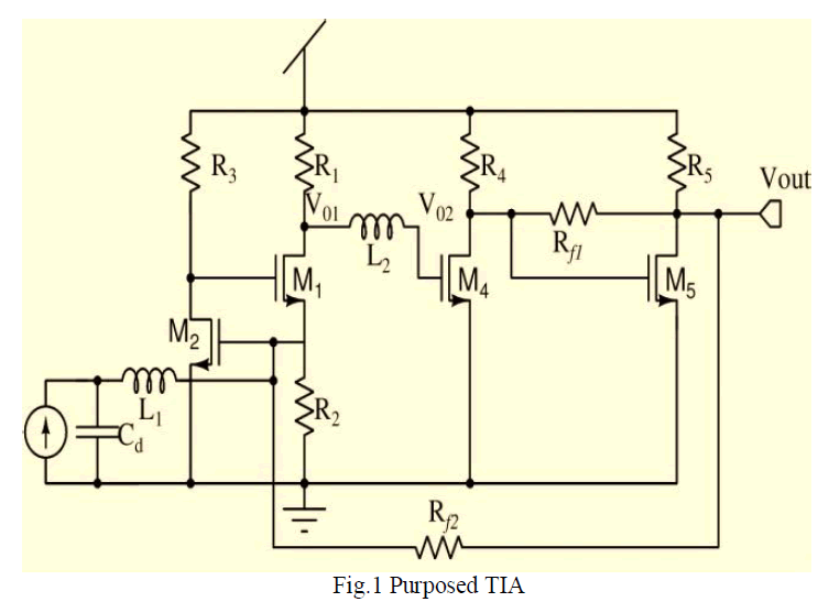 |
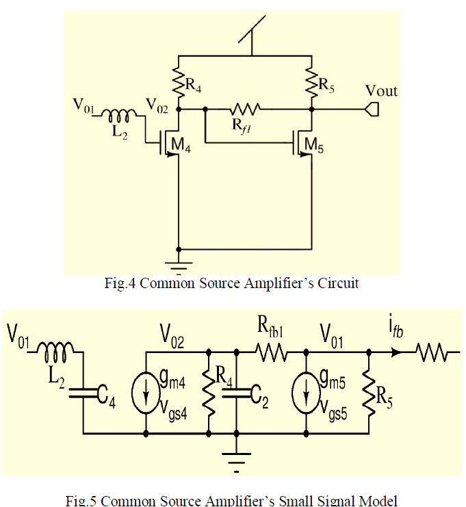
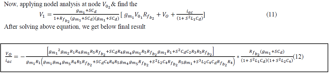
| Regulated Cascode Stage Network The Regulated cascode is widely used for broad-band TIA design in high-speed optical communication. In the proposed design a RGC network is inserted between the input of differential amplifier and photodiode to attain wide band response. RGC is essentially a common gate amplifier with a local feedback. In the proposed architecture as depicted in Figure2, transistor M2 with resistor R2 forms the local feedback of RGC amplifier. |
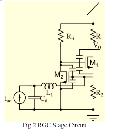 |
| It is Local feedback here in acts as a common source amplifier which gets a small portion of input signal and creates a voltage at the gate of M1. This signal is amplified at the output of M1. Moreover, it increases the effective transconductance of common gate structure which reduces the input resistance [7,8,9]. Reduction in input resistance isolates the input pole associated with large parasitic capacitance, Cpd from the bandwidth determination. As a result, the dominant pole of TIA is located within the amplifier rather than at the input node. To increase the bandwidth more, shunt peaking inductor LD1 and series peaking inductor LS1 are also incorporated in the RGC structure. These inductors are chosen similar to the technique described for the peaking inductors of differential amplifier. |
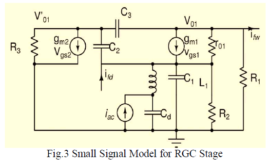 |
| the equivalent circuit diagram using small signal analysis method[3]. After applying the redefine capacitance, gate to source capacitance of MOSFET 1, gate to source capacitance of MOSFET 2 is denoted as C1 and gate to drain capacitance of MOSFET 2 is denoted as C2, and gate to drain capacitance of MOSFET 1 is denoted as C3. |
 |
 |
 |
| From equation12, we can say if we are doing proper tuning of inductor L1 and L2 then it is get poles in the pass band so we can able to maximize the bandwidth. There are know that the Gain Bandwidth product is constant, so we can put feedback resister Rfb1 and Rfb2 so we reduce gain and maximize operating frequency. The maximum frequency also dependent in MOSFET fabrication process Technology.The ïÿýïÿýïÿýïÿý of MOSFET dependent of Technology. In this design, these are using two negative feedback so it can enhance bandwidth. The operating bandwidth also dependent on the photo diode capacitor so it’s can resonant out that capacitor. The gain of circuit dependent of ïÿýïÿýïÿýïÿý of MOSFET which is dependent on size of MOSFET.If the size of MOSFET increasing then it is getting heavy input gate capacitance of MOSFET. So this design is optimize the size of MOSFET, inductor size, photo diode capacitor, feedback resistor. |
MEASUREMENT RESULTS WITH IMPROVE BANDWIDTH CHARACTERISTICS OF TRANSIMPEDANCE AMPLIFIER |
Simulation Environment |
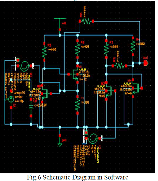
| The proposed TIA is designed in 130nm CMOS technology with 1.2 V supply voltage. RF NMOS and PMOS transistors are used for high frequency operation. The Photodetector capacitance is emulated using 60 fF MIM capacitor, and spiral inductors are used as peaking inductors. The whole system is characterized in SPECTRE/SPICE environment. |
Transimpedance Gain Responses |
| The SPECTRE/SPICE simulation of transimpedance gain response is shown in Figure7 Transimpedance gain response is investigated in three different scenarios - when there is no compensation, compensation with degenerating capacitance and feedback network and compensation with degenerating capacitance, feedback network, and peaking inductors. |
| The below figure 7 shows the gain variation with respect to frequency. In this we are using feedback resistors with large value. In this figure, we are marked at different gain. The first point shows gain from dc to 100MHz which is 66.56 dB. Due to pole placement we are able to achieve high bandwidth. |
 |
| The second point at 3.63GHz shows the gain at dip is 64.32dB due to effect of pole but it also cancel this pole with zero so the third point at 6.31GHz shows the overshoot and gain is 66.03dB. The forth point shows 3-dB cut-off frequency which is 7.5GHz. The above discussed result is using large value of feedback resistors or we can say this circuit is without feedback resistors. If it is using a low value resistor then it can found large bandwidth and less gain. |
| From below figure 8 it is seen that if we are using small feedback resistor then gain is dramatically decreases and 3dB bandwidth is slightly increases. So we can use variable resistors so we can manage gain as well as bandwidth according to requirement of application. |
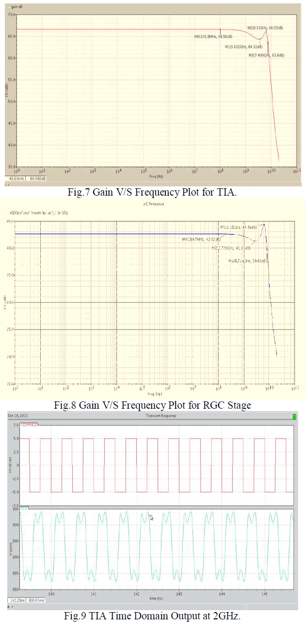 |
| The above figure shows that the input is applied is square wave pulse then the output is distorted because the high speed input is faded into circuit and output is not settled but next input pulse also applied so we can see distorted wave. The below figure shows clear picture of output settling |
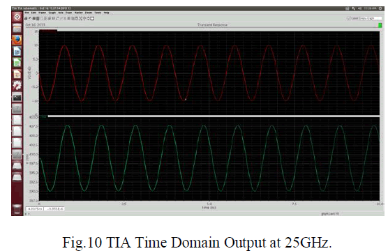 |
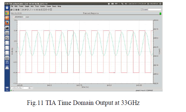
| the below figure shows if we are applying very high frequency the output not settled so we can show a nearly sinusoidal wave. If it is apply very high frequency the output is completely distorted and unable to detect output. |
 |
| For the variable gain and bandwidth requirement, it can use MOSFET as variable resistor. The many non idealities come into picture such as the finite quality factor of inductors, non-ideal behaviour of photo diode, and non-ideal performance of MOSFET etc. Due to non-ideal behaviour it is facing problems such as harmonics, poor phase noise, high leakage current etc. |
PERFORMANCE ISSUE FOR PROPOSED TIA |
| The CMOS technology using for designing TIA over the 130nm technology whose provide the high data speed in optical communication with 40Gb/s. These data rate can be achieving by improving the bandwidth & group delay of the Transimpedance amplifier without compromising remaining parameter like gain, figure of merit, power consumption etc. These TIA architecture achieves highest bandwidth and lowest group delay variation among all the TIA architectures. Input referred noise of proposed TIA is in between all of the architectures. Power consumption is the second lowest which also provides a decent figure of merit. |
CONCLUSION |
| The aim this work to design the new Transimpedance amplifier using 130nm CMOS technology. This work provides an overview of the existing transimpedance amplifiers in CMOS technology to enhance the bandwidth of TIA architecture so that it can be operated in 40 Gb/s data rate over the 10Gb/s data rate. It is also trade-offs between gain, bandwidth, noise, and group delay variation introduce severe hindrances to attain optimum performance of the TIA. |
| Different TIA architectures such as improved RGC, RTRN network, nested feedback etc. are studied in detail to improve the frequency response of the TIA. The proposed TIA is based on differential architecture with an RGC network as input and incorporating a feedback network and peaking inductors for bandwidth enhancement. Capacitive degeneration is also introduced to increase the number of zeros for better phase performance. Total system has been analysed for transimpedance gain response and noise performance. From simulation results, the proposed architecture shows excellent performance in terms of bandwidth and group delay variation with good transimpedance gain, input referred noise, and power |
References |
|