International Journal of Innovative Research in Computer and Communication Engineering
ISSN ONLINE(2320-9801) PRINT (2320-9798)
ISSN ONLINE(2320-9801) PRINT (2320-9798)
Prabhu.G1, Sridevi.A2
|
| Related article at Pubmed, Scholar Google |
Visit for more related articles at International Journal of Innovative Research in Computer and Communication Engineering
Clock mesh network is the repeated structure. Therefore network withstand any variations. The variations create clock skew in the circuit. But the skew is minimized in the clock mesh significantly because variation tolerant. The clock mesh networks mostly used in the high end products like microprocessors. Because mesh networks needs high resources compared to clock trees. The network needs more wire lengths and takes more area. In this paper, we present and construct initial mesh structure. The wire length and area minimized in the mesh structure. We try to implement clock mesh in the low end products like ASIC chips.
Keywords |
| Clock mesh optimization, clock mesh synthesis, robust clock networks, and variation tolerant clock network synthesis. |
INTRODUCTION |
| AS the VLSI technology continues to 65 nm and below, he effects of manufacturing variation, power supply noise, temperature variations, and so on, on clock skew are coming more significant. Clock network is especially sensitive to such variation effects, resulting in unwanted skews. Since higher skews directly reduce the maximum frequency of the circuit, reducing the clock skew variation can improve timing yield. Some of the approaches proposed to reduce clock skew variation are variation aware buffer/wire sizing, variation aware routing, link insertion in clock trees, and leaf level meshes. Among different methods suggested for skew variation reduction, the leaf-level mesh with a top-level tree has been shown to be very effective in reducing skew variation in several commercial chips as noted in and of its high redundancy, with multiple source to sink paths for every sink. A clock distribution network is typically the largest net in the circuit net list and operates at the highest speed of any signal within the entire synchronous system; hence the clock Network often takes a significant fraction of the power consumed by a chip. Clock waveforms must be sharp and noise-free since all the data signals are referenced by the clock signals. Technology scaling has made long global interconnect wires significantly more resistive as wires become thinner. In fact, the lack of research on automated clock mesh synthesis was noted as early as in 2001. However, no comprehensive work has been done on this important topic in the literature, to our best knowledge. Even in the recent tutorial on clock distribution networks, no systematic method has been presented for mesh planning1 or optimization. |
| Clock meshes a viable option for non-microprocessor chips, a fully automated framework for mesh planning, synthesis, and optimization is needed. Such a framework can enable chip teams to achieve a smooth tradeoff between performance (skew) and power (area). |
| It may be noted that fully automated clock mesh planning/ synthesis and optimization will be very useful to microprocessor chips as well. For example, automated mesh planning/synthesis can be used to get the preliminary clock mesh after which finer adjustments can be made manually. Similarly, mesh optimization can be performed on the individual grid zones2 to reduce power/resources used. The potential difference on the use of such automated methods between microprocessor and other chips lies in their respective resource vs. skew tradeoff. While microprocessors might opt for maximum power reduction with a strict skew requirement, other chips might opt for minimum skew with a strict power/resource target. |
LEAF-LEVEL MESH |
| This dissertation addresses variation and power issues in the design of current and potential future CDN. Nontree based distributions, on the other hand provide a high tolerance to variations due to the redundancy created by multiple paths between clock source and the sinks. One of the most widely used non-tree based CDN is clock mesh. Due to the high redundancy, mesh architecture offers high tolerance towards variation in the clock skew. However, such a redundancy comes at the expense of mesh wire length and power dissipation. Clock mesh usage is limited to high-end designs due to the significantly high resource requirements compared to clock trees and the lack of automatic mesh synthesis tools. Most existing works on clock mesh networks either deal with semicustom design or perform optimizations on a given clock mesh. However, the problem of obtaining a good initial clock mesh has not been addressed. Thus it can be overcome by designing good initial clock mesh. |
| Synchronous systems consist of sequential registers (latches, flip-flops) and combinational logic connecting registers. While the functional requirements of a digital system are satisfied by the register transfer level (RTL) and logic synthesis, the overall performance and timing constraints require insertion of pipeline registers to ensure that the latencies of critical paths between registers satisfy timing constraints. |
| Clock signals are delivered from a clock generator to sequential elements by a clock distribution network, which must optimize important parameters such as clock skew, slew rate, insertion delay, power dissipation, area and sensitivity to variations. |
| To ensure performance and reliability, proper design and effective optimization of clock distribution networks are crucial; therefore, clock network synthesis is excluded from other signal-net routing and processed by specialized |
A. Meshwork Framework |
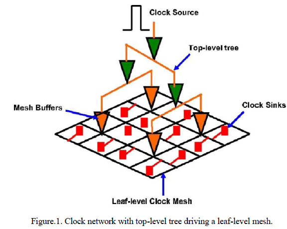
| In this paper, we attempt to address all these drawbacks. The below figure 1 shows clock network with top level tree. |
 |
| 1) Mesh planning and synthesis: a simple yet effective method for planning and synthesis of a buffered clock mesh for a given set of design constraints. This method can choose a good initial mesh, which can be further optimized for power/resource reduction. |
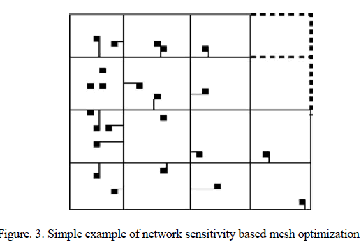
| 2) Mesh optimization: an efficient algorithm using network sensitivity theory to remove mesh edges with little impact on skew variability. This formulation is more accurate than the work of because the mesh delay sensitivities are directly considered during optimization. |
| 3) Buffer modeling for mesh optimization: an efficient buffer modeling method that is especially suitable for use during clock mesh optimization. |
| 4) Wire sizing for reliability: an effective heuristic that sizes relatively few mesh segments to meet the EM constraints of the optimized mesh. The above contributions make Meshwork the first comprehensive framework for complete automation of clock mesh. |
| Skew reduction is key to the top-level clock networks. Interconnect delays tend to dominate the cell delays, and with careful design, the clock is transmitted to the regional and local clock buffers with minimum delay variations. |
B. Total Wire length as a Function of Mesh Size |
| The wire length of the mesh itself is a linear function of mesh size. Let us now consider the effect of increasing the mesh size on the sum of wire lengths of all the stubs. As either m or n increases, a randomly chosen sink is more likely to have closer horizontal or vertical mesh segment. Since the maximum number of stubs is constant, it is very likely that the total stub length decreases. The vast majority of integrated circuits adopt a synchronous design methodology. Today, these systems contain billions of transistors which are broken into multiple components consisting of memory blocks, analog and mixed signal blocks, custom Digital blocks, sequential elements, and combinational cells. In synchronous design, a special signal called clock governs all operations and data transfers. The system functions properly when the clock is distributed over the design and arrives at the sequential elements ideally at the same time. Although this is not possible due a variety of design and technological reasons, the objective of the design is to distribute the clock to all sequential elements with the smallest delay possible. |
MESH PLANNING AND SYNTHESIS |
| The mesh planning and synthesis problem can be stated as follows. |
| 1) Given: sink locations and load capacitance, buffer library, Interconnect parameters, variation models, nominal/variational skew targets. |
| 2) Problem: obtain an initial clock mesh with minimum routing and buffering resources such that the given design constraints are likely to be satisfied. It shall be noted that our objective is not to get a final clock mesh, but to quickly get a good mesh that can further be optimized using the algorithm presented. |
| A. Total Wire length as a Function of Mesh Size: |
| Clock signals are particularly affected by this increased wire resistance, and precise control of clock-signal arrival times has grown in importance since they severely limit the maximum performance of the entire system. To ensure performance and reliability, proper design and effective optimization of clock distribution networks are crucial; therefore, clock network synthesis is excluded from other signal-net routing and processed by specialized algorithms and techniques prior to global routing of signal nets. |
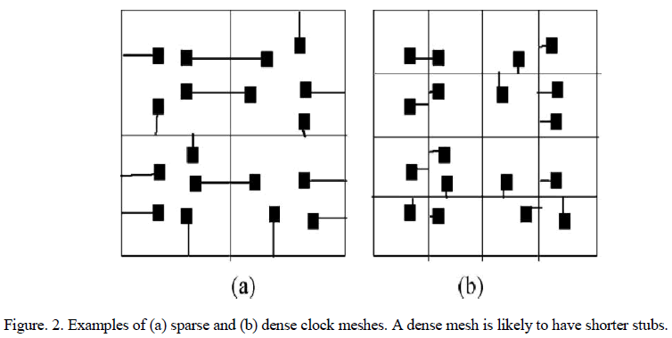
| The wire length of the mesh itself is a linear function of mesh size. Let us now consider the effect of increasing the mesh size on the sum of wire length of all the stubs. As either m or n increases, a randomly chosen sink is more likely to Closer horizontal or vertical mesh segment. Since the maximum number of stubs is constant, it is very likely that the total stub length decreases. In a sparse mesh, the mesh wire length is less when compared to the dense mesh than a dense mesh because each sink needs to be connected to the nearby mesh point using a longer interconnect. |
B. Skew as a Function of Mesh Size |
 |
| Skew variation is typically a decreasing function of mesh size because of two factors. First, the mesh itself becomes denser, resulting in more redundancy, making it more tolerant to variations. Second, the length of the stub also decreases, resulting in reduction of the maximum possible the maximal length of a wire that can be driven by an inverter started a steady decrease. This phenomenon boosted demands for repeaters in clock networks, raised their power profile, and complicated their synthesis. Research in delay-driven buffering of single signal nets arguably an easier problem and on a smaller scale has blossomed well into the late 2000s, leaving clock-tree synthesis a difficult, high-value target. |
| The first component is the skew due to the differential loading/sizing of the mesh buffers. This is the difference between the maximum delay of any buffer in the library under its maximum loading condition and the minimum delay of any buffer in the library under the maximum loading condition of the previous sized buffer (q−1). A previous sized buffer for a given buffer is the nearest smaller buffer when all buffers are sorted in ascending order of drive strength. We can consider a load of CLmax q−1 to be a lower bound of the load for buffer bq because we assume the smaller sized bq−1 will be used whenever the load is smaller than what buffer bq−1 can drive to save buffer area. |
| The second component is because of the difference in proximity of each sink to the buffer that is closest to it. Due to the redundancy of the mesh, this component will be usually small for a well-driven mesh satisfying the slew requirements. If Dmax is the maximum distance for a given buffered clock mesh, then maximum skew is equal to the delay in the segment itself. This corresponds to the worst case situation where a sink is located right next to a mesh buffer, while another is located at a distance of Dmax from the same buffer with all other components being identical. |
| The third component is due to the difference in the stub lengths and load capacitance. This component can be significant because it is uncontrolled by the redundancy of the mesh. It represents the worst case skew that can be caused when one of the sinks is located on the mesh itself and the other sink with maximum load capacitance is connected to the mesh using a stub of maximum length. The situation in which all the three factors discussed above might combine, resulting in maximum skew between two sinks. |
| For the first case, a big buffer drives a big load capacitance that is located at a distance Dmax from the buffer. For the second case, a small buffer drives a small capacitance located right next to it. |
| Among the skew components, the first component depends only on the buffer library and sets a practical limit on the skew obtainable using the given set of library buffers. The third component depends only on the mesh size and, hence, can be obtained for a given mesh size once. However, to accurately evaluate the second skew component, the precise location of mesh buffers should be known. But buffer locations cannot be known unless we choose the mesh size. Thus, there is a chicken and egg problem in accurate estimation of the second component. |
| For a given set of library buffers and slew requirements, as the mesh is made denser, there will be addition of more mesh buffers to satisfy the slew requirements. Thus, for a randomly selected sink, the location of the nearest buffer is likely to be proportionately closer as we increase the mesh density. |
| The value of scaling factor can be estimated based on a few experiments and used for estimating the skew bound subsequently. Though this approach is an approximation and we can find corner cases where this observation need not be true, our experiments on several benchmark circuits show that this assumption is valid in practice. Also, the choice of buffer placement/sizing algorithm influences the accuracy of this approximation. For example, if the buffer placement/sizing is done in such a way that buffers are placed close to sinks, then the second factor can even be neglected from skew bound analysis. Our buffer placement/sizing algorithm enables us to achieve that a variety of clock network topologies and deskewing techniques were developed for Microprocessors previously. The skew is the key parameters of clock networks in the microprocessors designed by IBM and Intel from the late 1990s to early 2000s. All those clock networks are regular, and only minimally adapt to sink locations. IBM S/390 used two-level balanced H-like trees. The clock network of the IBM Power4 processor consists of tuned H-trees driving a single full-chip grid. Active deskewing and wire-width tuning were employed to reduce skew. Alpha 21264 utilized hierarchical structures consisting of a global grid, six major grids and local clocks. The Intel Pentium series used spine (tall tree) structures driven by balanced binary trees. Adaptive deskewing technique based on a delay-locked loop (DLL) reduced skew from 100 ps to 15 ps in Pentium III. Deskewing by a 5-bit domain deskew register (DDR) was employed in Pentium 4. |
C. Mesh Optimization Friendly Buffer Placement/Sizing |
| The buffer insertion heuristic of two main drawbacks. First, the potential impact of buffer insertion on mesh optimization is not considered. This might result in buffer insertion at nodes that could have been optimized away if the buffer were not present. Second, the cost function used in the set-cover formulation of ignores the low-pass filter characteristics of an RC mesh. For an RC mesh, the attenuation of a ramp signal applied at a given node increases exponentially as a function of distance from the node. This attenuation is constant for a given clock frequency. Hence, inserting several small buffers distributed throughout the clock mesh instead of fewer big buffers might result in lesser buffer area and improve slew at the clock sinks. |
| The high-quality synchronous VLSI designs, clock network synthesis is becoming a more important problem as it significantly impacts the performance, area and power dissipation of the design. The trend of increasing system complexity in conjunction with architectural-level pipelining increases the number of clocked elements. Semiconductor scaling facilitates smaller cycle times, but this trend assumes increasingly reliable clock distribution. The design of clock networks directly influences the maximum operating clock frequency because it determines clock skew, slew rate and insertion delay of the clocked elements. Decreasing power consumption has become one of the main objectives in IC design today. |
| The two approaches to the design of reliable clock networks. First, one can use strong devices or thick wires that are less affected by variations. Second, one can build a redundant clock network with multiple paths from the clock source to each clock sink, or only some clock sinks. The impact of variation on one path can be compensated for by the clock signals from the other less-affected paths. In modern clock network design, this is mostly done by using mesh/grid type structures. However, neither method can avoid increase in total capacitance, which results in an increase in total power consumption. |
| Clock network synthesis for commercial designs is verified with respect to multiple process corners (or scenarios). Each corner represents a different operation environment of the chip and commercial clock network synthesis tools try to optimize the clock network based on multi-corner optimization. However, this multi-corner analysis cannot model intra die-process variations and decreases the accuracy of skew analysis as the impact of variations increases. One can utilize Monte-Carlo simulations for accurate estimation of the impact of variations, but this method is too time-consuming and remains impractical within clock network synthesis. Statistical timing analysis can model the impact of timing variations more efficiently, but remains relatively unexplored in the context of state-ofthe art clock network synthesis. |
| In a physical design flow, clock routing is performed after cell placement, which determines the physical locations of registers. Most academic/commercial placement tools do not distinguish clocked elements from combinational logic cells. Hence, even though it is possible to improve the quality of a clock network (especially in terms of power) by modifying the locations of registers, clock network synthesis techniques are often prevented from altering the locations of registers. Some researchers proposed techniques like leaf-level register clustering, but finding optimal register locations during placement remains an open challenge. The produced clock network will provide information on the latency and skew for each macro. This information can be used to drive the placement and optimization of the different partitions concurrently. |
EXISISTING APPROACHES |
| The design goals of a clock mesh implementation are shaped by the type of design, and the available timing and power budgets. Below are the most important design goals of designing a mesh. |
| Skew reduction is key to the top-level clock networks. Interconnect delays tend to dominate the cell delays, and with careful design, the clock is transmitted to the regional and local clock buffers with minimum delay variations. |
| The phenomenal growth of the semiconductor industry has made the design of integrated circuits a daunting task. A synchronous digital system is a popular design paradigm due to the ease and clarity of data communication between the different components of the system under design. However, due to the ever-increasing miniaturization of the design process, the high degree of integration which dramatically increased the number of clock elements, and the increase in the clock speed, the design of the clock network which is responsible for synchronization amongst the various design components has become very challenging. |
| Aggressive scaling has lead to increasing uncertainty in design due to process variations. Clock skew is one such design parameter that is very sensitive to process variations. The design of CDN could include multiple conflicts such as wire length, power, signal slew rate, skew rate, skew target, and tolerance of clock skew to variations. Tree based distributions offers the advantage of simplicity (single path between source and sinks) as well as lower wire length at the expense of skew tolerance, inserting buffers of uniform sizes across the clock mesh leads to the performance constraints such as power, speed, area, etc., clock mesh consumes a high area/power overhead, thus there is a need to address more efficient ways of designing/optimizing the clock mesh. The main disadvantage is that the clock skew reduces the expense of maximum permissible circuit delay. |
PROPOSED SYSTEM |
| We propose a set cover based algorithm for finding the mesh buffer locations and their sizes. Non tree based distributions provides a high tolerance towards process variations. The candidate locations and sizes of the buffers which are used to drive the clock mesh are presented using heuristic algorithms (set cover based algorithm). Therefore these algorithms work faster on a discrete library of buffer sizes. But the constraints in the existing techniques can be overcome by providing different sizing of buffers. So we present efficient post processing techniques to reduce the size of the mesh buffers after mesh reduction. Finally we make comparisons of wire length, power dissipation, nominal skew & variation skew using Xilinx software. |
| The clock mesh constraints are overcome by two processes. First a simultaneous buffer placement and sizing is done which satisfies the signal slew constraints while minimizing the total buffer size. The second one reduces the mesh by deleting certain edges, thereby trading off skew tolerance for low power dissipation and to be analyzed. |
A. Mesh Optimization Algorithm |
| The number of clock registers in the design is growing at an astounding rate. This puts a huge burden on the clock network and makes balancing it a formidable task. As the die area increases, the clock network has to stretch over the entire area with long wires. These long wires require careful planning and optimization to control their delays. In addition, the clock buffers that are needed on these long wires tend to be large cells which consume a lot of power and present large blockages to the place and route engines. |
| For high-speed designs, careful design and planning of the top-level clock networks key to a successful tapeout. Typically, microprocessor designs choose a mesh implementation of the clocks due to their aggressive timing constraints. Traditional zero-skew or near-zero skew clock tree synthesis engines cannot handle this task. However, clock meshes have not been favored in ASIC design styles due to the design cost associated with them. Mesh topologies consume more power and areas compared to trees. Microprocessors, in general, enjoy a bigger design budget for power and other resources as compared to ASICs. For example, microprocessor designs can dedicate special design teams with circuit design expertise to tackle the clock design problem. |
| They can afford to dedicate special routing layers forth clock if needed to insure robust and high-performance implementation. However, ASIC designs typically do not have this expertise available and cannot afford such high costs due to the tight budget under which they operate. |
B. Buffer-Resizing for Mesh Optimization |
| A key drawback is that the optimized mesh uses the same buffer placement/sizing as the initial mesh. This can result in buffer area and power wastage. In this paper, we propose an efficient buffer resizing heuristic to reduce the buffer area/power for a given optimized mesh. The main steps in our approach are as follows. |
| 1) For each clock buffer, obtain the rectangular covering region in the mesh where the total capacitance (including sink capacitance) is less than buffer load limit under the given slew constraint. |
| 2) For each buffer that has an overlap with another buffer, consider resizing to the previous sized buffer such that the total covering region for all clock buffers is maintained. |
| 3) For each buffer that has an overlap with another buffer, consider resizing to the previous sized buffer such that the total covering region for all clock buffers is maintained. |
| 4) Repeat this process till there exists no buffer that can be sized down without reducing the total coverage. The amount of buffer area reduction obtained by the above heuristic is proportional to the reduction in mesh wirelength. However, the proportional reduction in power is likely to be less because the redundant buffers in the optimized mesh were driving light loads. |
 |
SIMULATION AND RESULTS |
| A grid is composed of a custom-designed buffer configuration and a grid of wires. In high-speed designs, the grid is designed, sized and laid-out after several iterations of circuit simulation based on estimates of the iteration die size, the interconnect delay, and the total load capacitance. Several generations of DEC’s Alpha microprocessors used this topology in their designs as shown in above figure. The clock mesh network has low skew variation by design but the major drawback is its high power dissipation. Different methodologies are proposed in recent years for reducing the power dissipation on the clock mesh network. |
| Clock mesh or grid is the favored clock distribution topology in microprocessors and other high-end designs. The redundant nature of the mesh makes it more immune to on-chip process variations. |
| It is critical that the clock network be shielded from any source of noise. As mentioned earlier, not only is the clock the biggest contributor to noise in the design due to the high rate of switching, but also it is the most sensitive signal since it is the gateway for any data transfer in the design. The best way to shield the clock network is to concurrently design it with the power network, and have the clock wires be shielded by the neighboring power wires. This would enable reliable power design as well as robust clock. |
| A. Blockages |
| An important issue to be considered during clock network synthesis is the presence of blockages. The MeshWorks framework can work seamlessly even for chips with blockages. This is because the mesh optimization problem with blockages is identical to the optimization problem obtained by replacing the blockage with only the clock pins of the blockages connected to the mesh. Since the area of the blockage will not have any other clock sinks, the mesh segments within this area will naturally get optimized away. |
| B. Multi-Clock Floor plans |
| One of the main reasons why clock meshes are not used even in high performance ASICs is that they typically require multiple clocks to interact heavily and so they will have sinks of multiple clocks interspersed in the same floor plan. As a result, using a mesh structure for the clocks will require two separate meshes covering the entire floor plan, which is obviously unaffordable due to power/resource constraints. |
| C. HIGHLY UNEVEN LOAD DISTRIBUTION |
| The practically significant issue of uneven load distribution in different parts of a large chip can be addressed effectively using the MeshWorks framework. Such a situation can happen in reality when different IPs from different vendors are merged to create large system-on-a-chip designs. Even in situations like this, the MeshWorks framework can be used effectively. One method is to start the mesh optimization with a dense mesh that will work for the densest region of the chip. Since our method will automatically optimize away unnecessary edges that do not contribute to skew variation tolerance, the mesh segments in the regions with light load distribution will be optimized away naturally. |
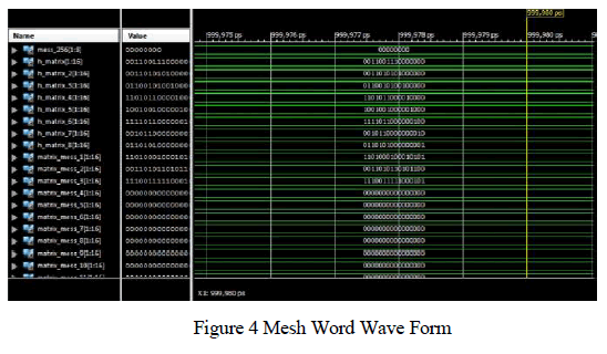 |
| The algorithm is implemented in VHDL language Xilinx and the effectiveness of the algorithm is validated. The mesh network can be either considered as an array or as a matrix. Each elements of the matrix can be considered as nodes of the mesh network. The resistance and capacitance values of the link are given as inputs. All the delay values are also given. |
| After giving the inputs, the matrix values for each edge pairs are calculated using the stored matrix values in the system. The unity matrix value is compared with given value. The matrix mesh word can be formed for each combination. The give input combination can be tested using c_ht_out in the waveform. |
CONCLUSION |
| The research work has been focused on sizing the interconnect elements within the clock mesh. We believe that sizing the interconnect wire segments of the clock mesh and the buffers driving the mesh simultaneously would yield more improvement in the power of a clock mesh area satisfying the constraint. The work presented here can be easily extended for sizing buffers and mesh elements simultaneously. Since, our design techniques are faster; it offers the flexibility to optimize clock mesh with different design objectives. The slew constraints are also satisfied while minimizing the total buffer size in a simultaneous buffer placement and sizing module. Xilinx ISE simulation results were implemented using cell library based technology. Thereby trading off skew tolerance for low power dissipation has been achieved. The results also show that the links added by the proposed algorithms are considerably shorter on the average, thereby making the non-tree more routable than the results of the existing algorithms. The new algorithms are particularly attractive as they scale extremely well to big clock networks, i.e., the bigger the clock network, the less overall link cost. This technique is used mainly for ASIC designs because clock skew problems are highly discrete for ASIC clock networks. |
| The mesh structure is implemented in VHDL algorithm. This algorithm is simulated Xilinx ISE with QSIM. |
References |
|