International Journal of Innovative Research in Computer and Communication Engineering
ISSN ONLINE(2320-9801) PRINT (2320-9798)
ISSN ONLINE(2320-9801) PRINT (2320-9798)
Somya Goel1, Dr Ranjit Singh2, FIETE
|
| Related article at Pubmed, Scholar Google |
Visit for more related articles at International Journal of Innovative Research in Computer and Communication Engineering
The present paper proposes a design and implementation of 2.4GHz-band Zigbee transreceiver for an acknowledgement frame. The behavior of digital transreceiver is modeled using VHDL. The code is then synthesized, simulated and implemented on Vertex-2P FPGA. Improvement is attained in terms of performance and chip-area. The Zigbee transreceiver design meets theoretical expectations.
Keywords |
| VHDL, Zigbee Transreceiver, FPGA, Acknowledgement frame |
INTRODUCTION |
| The emergence of wireless interface devices created a strong demand for low-data-rate short-range wireless networking. This led to the development of Zigbee standard, which is a set of new communication protocols for wireless transmission [1]. The Zigbee standard is developed by the Zigbee Alliance [2], which has hundreds of member companies, from semiconductor industry and software developers to original equipment manufacturers and installers. The Zigbee Alliance was formed in 2002 as a nonprofit organization open to everyone who wants to join [3]. The Zigbee standard has adopted IEEE 802.15.4 as its Physical Layer (PHY) and Medium Access Control (MAC) protocols [4]. Hence, a Zigbee device is compliant with the IEEE 802.15.4 standard as well. The PHY layer supports three frequency bands: a 2.45 GHz band with 16 channels, a 915 MHz band with 10 channels, and a 868 MHz band with 1 channel. |
| Main network topologies used in ZigBee wireless networking are star and peer-to-peer networks. These topologies can be used in different environments and situations. In the star topology, every device in the network can communicate only with the personal area network (PAN) coordinator. A Full Function Device (FFD) takes up a role as PAN coordinator; the other nodes can be „Reduced Function DeviceâÃâ¬ÃŸ (RFDs) or FFDs. In the peer-to-peer topology, each device can communicate directly with any other device if the devices are close enough together to establish a successful communication link. Any FFD in this topology can play the role of the PAN coordinator [3]. |
ZIGBEE TRANSRECEIVER |
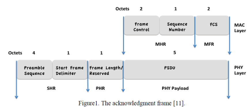
| MAC frame structures consist of beacon, data, acknowledgment, and MAC command frames. The beacon frame is used by a coordinator to transmit beacons. The function of beacons is to synchronize the clock of all the devices within the same network. The data frame is used to transmit data. Meanwhile, the acknowledgement frame is used to confirm successful frame reception [4]. The MAC commands are transmitted using a MAC command frame. The Zigbee digital transmitter is designed for an acknowledgment frame which is shown in Figure 1 based on IEEE 802.15.4 standard. |
| This is the simplest MAC frame format and does not carry any MAC payload. This frame is constructed from MAC header (MHR) and MAC footer (MFR). The frame control field and direct sequence number (DSN) form the MHR. The MFR is composed of 16-bit frame check sequence (FCS). Both MHR and MFR also known as PHY service data unit (PSDU), which becomes the PHY payload. The PHY payload is prefixed with the synchronization header (SHR), comprised of preamble sequence, start of frame delimiter (SFD), and PHY header (PHR). Together with the SHR, PHR and PHY payload form the PHY protocol data unit (PPDU). length of preamble sequence field is 4 octets. As for SFD, the length is 1 octet. The PHR also contains 1 octet. This is follows by the MHR and the MFR with 3 octets and 2 octets, respectively. Hence, the acknowledgment frame length is totally 11 octets. |
 |
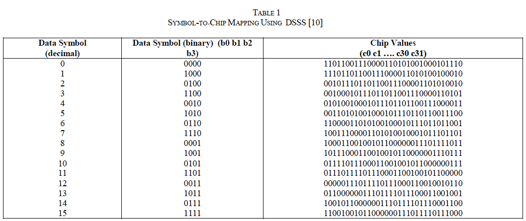
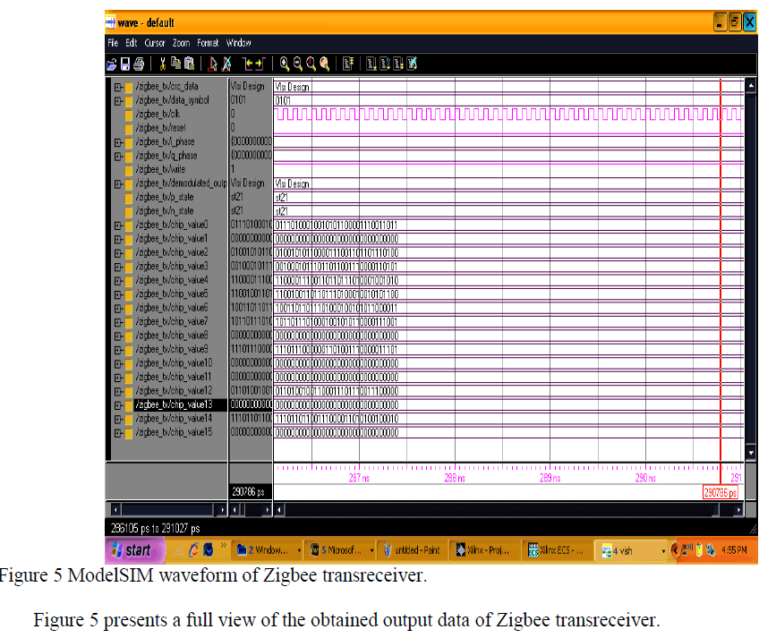
| IEEE 802.15.4 standard employs direct sequence spread spectrum (DSSS) that uses a digital spreading function representing pseudo-random noise (PN) chip sequences as shown in Table 1 [9]. The acknowledgment frame used in this paper contains 11 octets (88 bits) of physical protocol data unit (PPDU). Figure 3 shows the architecture of the proposed Zigbee digital transmitter. Binary data from the PPDU packet are inserted into the cyclic redundancy check (CRC) block to detect errors during transmission. CRC is the most preferred method of encoding because it provides very efficient protection against commonly occurring burst errors [3], and is easily implemented [4]. |
| CRCâÃâ¬ÃŸs can detect all one bits and two bits errors as well as all odd number of bits in error [5]. Since CRC is a technique for detecting errors, but not for making corrections when errors are detected, the whole packet data will be retransmitted if error occurs [6]. For Zigbee Standard, CRC involves a division of the transmitted packet data by a constant called the generator polynomial [7]. In this paper, the CRC block contains the SHR, PHR and PHY payload. In the PHY payload, the FCS mechanism employs a 16-bit CRC in order to detect errors [4]. The FCS is calculated over the MHR and MFR payload parts of the frame using the algorithm. |
 |
| Then, every four bits of each PPDU octet are mapped onto one data symbol. The mapping takes place in a bit-tosymbol block. The 4 least significant bits (LSBs) (b0, b1, b2, b3) of each octet is mapped into one data symbol and the 4 most significant bits (MSBs) (b4, b5, b6, b7) of each octet is mapped into the next data symbol. Each octet of PPDU is processed through the bit-to-symbol block sequentially, beginning with the Preamble field and ending with the last octet of the PSDU. |
| The proposed digital transceiver for Zigbee applications is shown in Fig 2. The acknowledgment frames which is originated from MAC sub-layer is inserted into the CRC block. Then, every 4 bits are mapped into one data symbol in the bit-to-symbol block. The symbol-to-chip block performs the DSSS where each symbol is mapped into a 32-chip PN sequence. After that, these chips are processed by OQPSK (Offset Quadrature Phase Shift Keyed) modulator and the half-sine pulse shaping block to reduce inter-symbol interference. The resultant signal is transmitted and received by OQPSK demodulator, follows by chip synchronization and de-spreading blocks to regain the original data bit. |
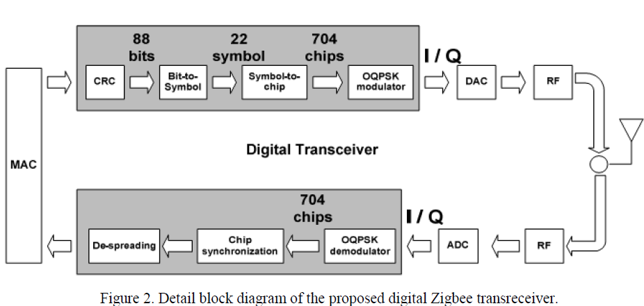 |
| A symbol-to-chip block follows, and utilizes a DSSS method to map each symbol to a unique 32-chip PN sequence [1]. The IEEE 802.15.4 uses this method to improve the receiver sensitivity level and increase the jamming resistance [1]. The DSSS method is also necessary in improving receiver performance in a multi-path environment because in most practical scenarios, the transmitted signal may find several different paths to the receiver due to reflections, diffractions and scatterings. These signals have different delays and phase shifts; therefore, the summation will be a distorted signal [7]. The signal quality may become poor and this can result in poor communication. Finally, OQPSK method is applied to the chips. |
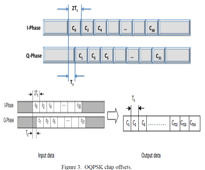
| OQPSK modulator is the improved version of QPSK. This method processes the in-phase (I) signal with a quadrature phase (Q) signal, and delayed by half a cycle to avoid sudden phase-shift changes [8]. As shown in Figure 5, to form the offset between I-phase and Q-phase chip modulation, the Q-phase chips shall be delayed by Tc with respect to the Iphase chips. Tc is the inverse of the chip rate. The chip rate is nominally 2 Mchip/s which is 32 times the symbol rate [8]. The resultant signal is then amplified and transmitted. |
 |
DESIGN METHODOLOGY |
| The behavior of the Zigbee digital transmitter can be modeled using VHDL through Xilinx ISE. The VHDL module for each transmitter can be combined, then synthesized, simulated, and implemented on Virtex-2P FPGA. A logic analyzer verified that the design output waveform would match the simulation waveform. FPGA was adopted due to its parallel architecture and flexibility in implementation [9]. The proposed transmitter design method based on the behavior of each block is as follows. |
| The input data comprise 22 symbols. Each data symbol from the bit-to-symbol block is mapped onto a 32-chip PN sequence using the DSSS method. The output data are 704 chips in total with the frequency of 2 MHz. The numbers of chips produced are based on |
| [88 bits/4] symbols x 32 = 704 chips (1) |
| With the same frequency, each chip of input data is processed based on |
| output_data [2 * k - 1] = I_phase [2 * k - 2] (2) |
| output_data [2 * k] = Q_phase [2 * k - 1] |
| where 1 ≤ k ≤ 352. |
| Based on this equation, each even chip of output data is registered as C0, C2 ….. C704, and each odd chip is registered as C1, C3 …C703, which is totally 352 chips each for I-phase and Q-phase. These data chips will be the input for the next block in the Zigbee receiver. |
| The input data are composed of 704 chips and the frequency is 2 MHz. In this block, each even-indexed chip is modulated onto the I-carrier, whereas each odd-indexed chip is modulated onto the Q-carrier. The Q-phase chips are delayed by Tc with respect to the I-phase chips to form the offset between I-phase and Q-phase chip modulation. The output data consists of 352 chips for I-phase and Q-phase, respectively. |
| The value of Tc is calculated as follows: |
| Tc = 1/fOQPSK = 1/(2 MHz) = 500,000 ps. |
RESULTS AND DISCUSSION |
| Simulation and verification were performed for the Zigbee Transreceiver. |
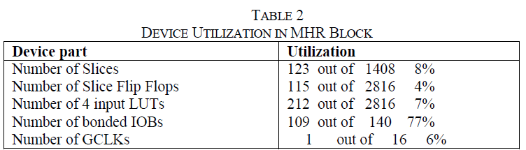
| A. Device utilization and timing summary of MHR (MAC Header) block |
| Device utilization is the hardware and logic circuitry required to implement the design. It consists of number of slices, flip flops, gates, combinational logic circuitry and input/output blocks. Selected Device: Selected Device: 2vp2fg256-6 |
 |
| 1) Timing Summary: Speed Grade: 6 |
| Minimum input arrival time before clock: 5.214ns |
| Maximum output required time after clock: 4.483ns |
| Total memory usage is 81080 kilobytes |
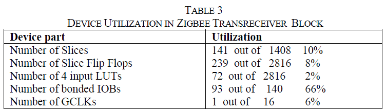
| B) Device Utilization and Timing-Summary of Zigbee Transreceiver Block |
| Selected Device: 2vp2fg256-7 |
 |
| 1) Timing Summary: Speed Grade: -7 |
| Minimum period: 1.098ns (Maximum Frequency: 910.747 MHz) |
| Minimum input arrival time before clock: 4.381 ns |
| Maximum output required time after clock: 4.088 ns |
| Total memory usage is 82104 kilobytes. |
C) Simulation Waveform |
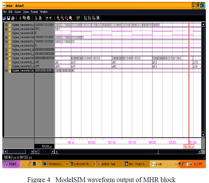 |
| Figure 4 presents a full view of the obtained output data of MHR block. The functional simulation depends on the test inputs in design. |
| Step input 1: reset = 1, clock is used for synchronization and then run. |
| Step input 2: reset = 0, same clock is used for synchronization. Force the value of crc_data [87: 0] = 88 bits value and run we will get the data in data_symbol , chip_value0[31:0] of 32 bits to chip_value15[31:0] of 32 bits . Get result i_phase[15:0] and q_phase[15:0] of 16 bits. |
 |
CONCLUSION |
| The VHDL code was synthesized, simulated, and implemented successfully on Virtex 2P FPGA. A pattern generator and a logic analyzer were used to stimulate the input data of 72 bits and to measure output data, respectively. The functionality of the proposed transmitter matches its theoretical expectation. With VHDL, the transmitter design area could be reduced to a smaller scale. Implementing the design of Zigbee digital transmitter on ASIC using 0.18 μm technology process is intended in the near future. With ASIC, the design core can be manually resized to obtain a smaller core area compared to FPGA. The transmitter will be implemented with a low sampling frequency and lower power supply at 1.8 V. |
ACKNOWLEDGMENT |
| The first author acknowledges financial support provided by Hi-tech Institute of Engineering and Technology, Ghaziabad 20001, UP, India. The second author acknowledges Ajay Kumar Garg Engineering College, Ghaziabad for providing inspiring and propitious academic ecosystem and facilities. |
References |
|