International Journal of Advanced Research in Electrical, Electronics and Instrumentation Engineering
ISSN ONLINE(2278-8875) PRINT (2320-3765)
ISSN ONLINE(2278-8875) PRINT (2320-3765)
S.Ramesh1, D.Suresh1, A.SyedAlthaf Hussain1,D.Tamilvanan1,M.P.Prabakaran2
|
| Related article at Pubmed, Scholar Google |
Visit for more related articles at International Journal of Advanced Research in Electrical, Electronics and Instrumentation Engineering
In this project we are going to design a low-cost of Video transmission through optical wireless communication. A 10Mbps optical transmission for free-space optical video data communication is presented. A channel-adaptive video streaming scheme which adjust video bit rate according to channel condition and transmit video through a hybrid free space optical (FSO) laser communication system. It has been shown that the proposed structure is suitable for uninterrupted transmission of videos over the hybrid wireless network with reduced packet delays and losses even when the received power is decreased due to weather conditions. By employing easy-to-find electronic components, the design consists of three main parts namely interface circuit, transmitter and receiver. The transmitter based on a simple inverter circuitry, drives a laser diode emitting 635nm visible red light. The incoming light signal is focused via 10-cm-diameter lens onto a photodiode SFH203. The received signal current from the photodiode is converted to signal voltage by a resistive-feedback trans-impedance amplifier, differentiator, and limiting amplifier and consequently delivered to the interface circuit. 10Mbps Ethernet link between two personal computers situated 100 meters apart has been successfully tested.
Keywords |
| Free space optical (FSO), Video Transmission, interface circuit, optical communication. |
INTRODUCTION |
| Laser wireless, also known as free space optics is a method of communication that involves using a light source, usually a laser, to transmit information through space or the atmosphere to a receiver. Optical wireless communication is an effective high bandwidth communication technology serving commercial point –to- point link in terrestrial last mile application, such as air-to-air, satellite-to submarine, air- to- satellite, and satellite-to satellite links, have several attractive characteristic such as dense spatial rescue, low power usage license free band of operation, and relatively high bandwidth[1,2,3]. Optical wireless communications (OWC) have attractive attention from many researchers worldwide for their potential advantages over radio links. |
A. Aim of the project |
| The Video transmission through optical wireless communication link using a LASER is to create a new form of optical communication to society the can be marketed with small size and low cost. The link consist a transmitter and a receiver both of which are battery powered and permanently fixed. The transmitter circuitry takes in a data stream of âÃâ¬Ãâ¢1s (+5V)âÃâ¬Ãâ and âÃâ¬Ãâ¢0s (0V)âÃâ¬Ãâ and then modulates the current through an LASER. The LASER sends photons with intensities proportional to input data bits across the Video transmission through Optical wireless communication link to a PIN photo-diode. The PIN diode is connected to the receiver which converts Optical power into an Output voltage. The size of each module is approximately the same and should accommodate all components needed to function. The LASER, PIN diode, and other circuitry will be able to operate off of portable battery due to low power consumption. Inexpensive parts and low power consumption present a lower marketing cost. Optical wireless communications (OWC) have attractive attention from many researchers worldwide for their potential advantages over radio links. Optical wireless links also offer high data rates, immunity to electromagnetic interference, and relative security since it does not penetrate walls [4, 5].The first is a short range application, such as, sending data from a computer, and this application has a data transfer rate range up to 10 cm. The second application (Audio) sends data at 25 Mb/s at a range up to 100 m, and this application could apply to a central classroom module sending data to laptops or PDAs of 100 Mb/s at a range up to 10 cm. The second application sends data at 25 Mb/s at a range up to 100 m, and this application could apply to a central classroom module sending data to laptops. |
B. Motivation |
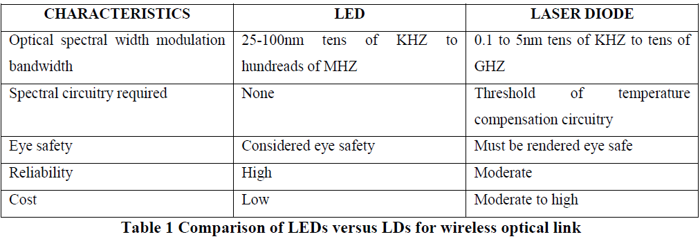
| The current form of Video transmission through optical wireless communication using light emission resides in the realm of LED and RF communication. The drawback to using LED and RF communication is output beam is incoherent, coupling efficiency is very low when comparing to LASER. The output power for LED is very low. The data rate of LASER is high when compare to LED. |
C. Background |
| The current wireless technologies such as Bluetooth, Wi-Fi, have low data transmission rate compared to that optical wireless communication. The data rate for optical systems is in the Gbps range. However, this technology is very expensive preventing it from replacing the current wireless networks such as Wi-Fi, RF communication. LASERs were proposed to replace the LED as the light sources in order to maintaining the high-speed data rate. |
D. Project Description And Goal |
| The controlled conditions are defined as the Video transmission through optical communication link maintain with 50 cm and operated in free space. The test will be conducted without excessive light such as sunlight. The LASER link is designed to transmit data bits from voltage generated to an oscilloscope through Free space optical communication using light from an LASER. The laser operates in the spectral range of infrared(above 650 nm in wave length).A PIN photodiode is employed on the receiver circuit to collect the light send from the transmitting LASER. |
SYSTEM DESIGN |
A. Methodology |
| The proposed system consists of three major units. They are: |
| - Transmitter Unit. |
| - Channel Unit. |
| - Receiver unit. |
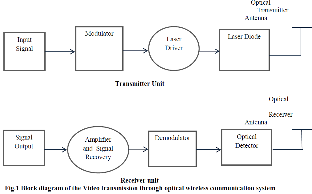 |
B. Transmitter Unit |
| Input signal, modulator, LASER drive circuit, LASER diode. For the transmitter we have the modulator which modulates of the input signal. This modulation can be software or hardware. The driver is necessary to transmit the signal to the LASER in the right frequency and amplitude. Newly developed high powers LASER emits substantial light and are typically very inexpensive. Currently, LASER can emit up to several watts of power into an angle of several tens of degrees. The lens collimated allow efficiently collimate the light into a determinate beam with more precision. |
C. Modulation |
| Optical modulation is one of the keys for realizing such high performance optical network. Digital communications employing LASER as optical carriers generally having carrier frequencies in the Megahertz range that permit enough high modulation bandwidths for video transmission. The optical modulation is used to modulate a beam of light, converting the electrical signal array into the light signal array and including information into the signal. |
D. Laser Driver Circuit |
| Drive circuits for laser diodes are either automatic power control (APC) circuits that maintain a constant light output power or automatic current control (ACC) circuits that maintain a constant current. The output power and wavelength of the laser diode can be affected by the changing of temperature. APC circuits provide a constant light output power despite variations in ambient temperature. If you have a DC power supply which provides you an accurate and stable DC voltage. You may use this APC circuit board without voltage regulator. |
E. Laser Diodes |
| Laser diodes (LDs) are a more recent technology which has grown from underlying LED fabrication techniques. LDs still depend on the transition of carriers over the band gap to produce radiant photons; however, modifications to the device structure allow such devices to efficiently produce coherent light over a narrow optical bandwidth LDs exhibit a second form of photon generation process: stimulated emission. In this process, photons of energy Eg are incident on the active region of the device. In the active region, an excess of electrons is maintained such that in this region the probability of an electron being in the conduction band is greater than it being in the valence band. The emitted photons in this process have the same energy, frequency, and phase as the incident photon. The output light from this reaction is said to be coherent [6,7,8]. |
 |
F. Channel Unit |
| The medium between transmitter and receiver unit is channel. The noise is added at channel. |
G. Additive White Gaussian Noise |
| Additive white Gaussian noise (AWGN) is a channel model in which the only impairment to communication is a linear addition of wideband or white noise with a constant spectral density (expressed as watts per hertz of bandwidth) and a Gaussian distribution of amplitude. The model does not account for fading, frequency selectivity, interference,nonlinearity or dispersion. However, it produces simple and tractable mathematical models which are useful for gaining insight into the underlying behavior of a system before these other phenomena are considered. Wideband Gaussian noise comes from many natural sources, such as the thermal vibrations of atoms in conductors (referred to as thermal noise or Johnson-Nyquist noise), shot noise, black body radiation from the earth and other warm objects, and from celestial sources such as the Sun. |
H. Receiver Unit |
| The receiver detects the light via the photo detector. The low current signal triggers a dual gate transistor (BF988), The detector is a photodiode, a type of photo detector capable of converting light into either current or voltage, depending upon the mode of operation. COTS photodiodes such as avalanche photodiodes (APDs) can be used as detectors, which can respond to pulses as narrow as several nanoseconds. The photodiode needs to have a balance between speed and sensitivity. The signal processing stage takes the current from the photodiode. This is pre amplified by a transimpedance amplifier (TIA). After that, the signal is filtered, amplified and processed. The demodulator realizes the demodulation of the input signal. This modulation can be software or hardware.This takes the current from the 12 V rail and transmits it to the NE592 video amplifier. The NE592 cleans the incoming rounded signal to a square wave. Pin 8 of the NE592 is the other part of the differential output and carries the data stream through a pre-amp circuit consisting of a pair of common emitter connected transistor. |
I. Photo Detectors |
| Photo detectors are solid-state devices which perform the inverse operation of light emitting devices, i.e., they convert the incident radiant light into an electrical current. Photo detectors are essentially reverse biased diodes on which the radiant optical energy is incident, and are also referred to as photodiodes. The incident photons, if they have sufficient energy, generate free electron hole pairs. The drift or diffusion of these carriers to the contacts of the device constitutes the detected photocurrent. Inexpensive photo detectors can be constructed of silicon (Si) for the 780–950 nm optical bands. |
HARDWARE DESIGN |
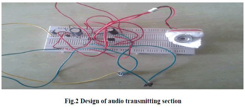
A. Audio Transmitter Section |
| The transmitter circuit (Fig.2) comprises condenser microphone transistor amplifier BC548 (T1) followed by an op-amp stage built around μA741 (IC1). The gain of the op-amp can be controlled with the help of 1-mega-ohm photometer VR1. The AF output from IC1 is coupled to the base of transistor BD139 (T2), which, in turn, modulates the laser beam. The transmitter uses 9V power supply. However, the 3-volt laser torch (after removal of its battery) can be directly connected to the circuit—with the body of the torch connected to the emitter of BD139 and the spring-loaded lead protruding from inside the torch to circuit ground. |
 |
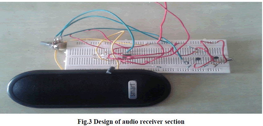
B. Audio Receiver Section |
| The receiver circuit (Fig. 3) uses an NPN phototransistor as the light sensor that is followed by a two-stage transistor preamplifier and LM386-based audio power amplifier. The receiver does not need any complicated alignment. Just keep the phototransistor oriented towards the remote transmitter’s laser point and adjust the volume control for a clear sound. To avoid 50Hz hum noise in the speaker, keep the phototransistor away from AC light sources such as bulbs. The reflected sunlight, however, does not cause any problem. But the sensor should not directly face the sun. |
 |
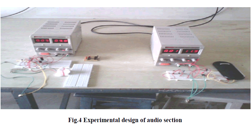
C. Experimental Result |
| This project has been finished with entire objective that we have planned. Transmitting the audio signal using free space optical communication has been successfully implemented and here the audio signal is given in the transmitter and the data (i.e. voltage) is monitored at the receiver side. . |
 |
VIDEO HARDWARE DESIGN |
| The hardware section is divided into three subsections as follows: |
| - Video circuit |
| - Max 232 |
| - Power supply unit |
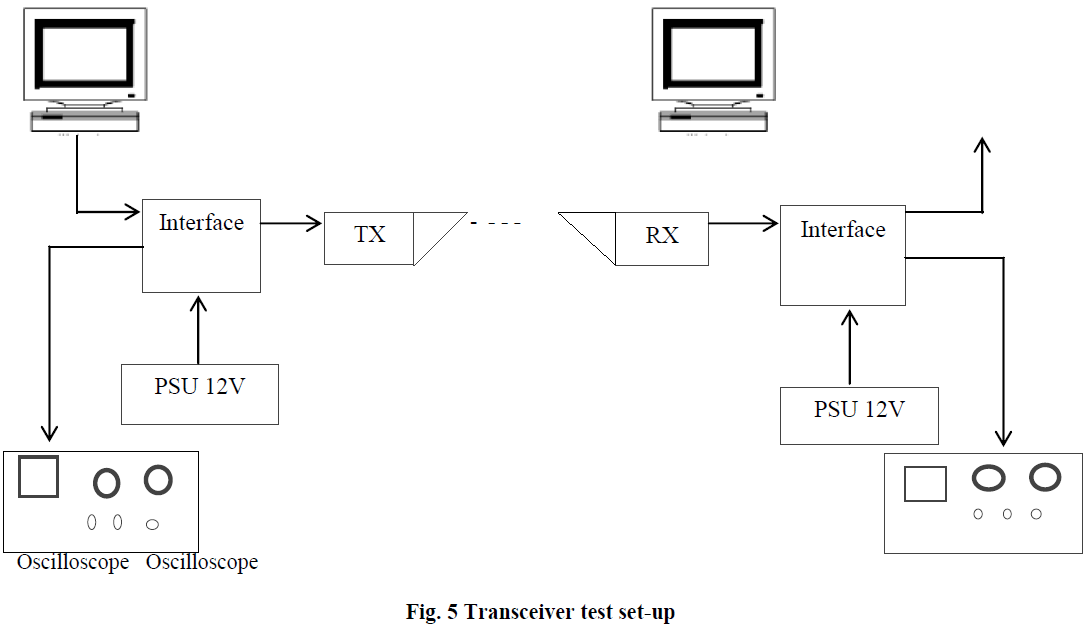 |
A. Interface Circuits |
| Interface circuit provides signal conditioning and generating some specific signals in order to comply with IEEE 802.3 standard. It can be divided into two major parts: (b) circuit that interfaces with transmitter and (c) circuit that interface with receiver |
B. Transmitter Interface Circuit |
| Transmitter interface circuit converts differential signals TD+, TD- from Ethernet card to a single signal and send to the transmitter by employing DS26LS32 chip. Moreover, it also generates 1MHz square wave while no data packet is being transmitted in order to comply with IEEE 802.3 standard. This signal will also be useful for the transceiver aiming during installation process. |
C. ReceiverInterface Circuit |
| Receiver interface circuit retrieves a single-end signal from the receiver and converts it to differential signal RD+, RDfor Ethernet card using DS26LS31 chip. While there is no data coming from the transmitter on the other end, the transmitter interface circuit produces a specific pulse signal for the Ethernet card following IEEE 802.3 standard. |
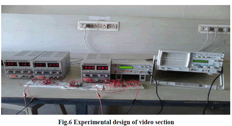
D. Experimental Result |
| This project has been finished with entire objective that we have planned. Transmitting the video signal using free space optical communication has been successfully implemented and here the video signal is given in the transmitter and the data (i.e. voltage) is monitored at the receiver side. |
| A video signal is given to the transmitter side, there with suitable modulation the signal is fed to the red laser. The laser transmits the signal which is received by the photo diode receiver and display on a computer which is interfaced with a Max 232 |
 |
CONCLUSION |
| The project was successful according to the initial goals of the project. A link was achieved at a distance of 30cm. Initially the proposal included a link with a slower data rate and a longer range and a link with a faster data rate and a shorter range. In the final product it was discovered that the link range had little effect on the overall performance. It is possible to achieve greater speeds with future revisions of both the driver and receiver boards. Link alignment should be studied further to achieve a more reliable data transfer at wider angles. It is also possible to achieve better results by using visible red light LASER and PIN. Also, the pre-bias and modulation currents should be studied using the evaluation board and the custom receiver to determine if it is possible to further reduce thermal noise created by the LASER. A package should be created in which an internal power supply (battery), casing, and lens are integrated. It will also be necessary to interface the transmitter and the receiver with a data source and memory such as USB and a hard drive. The receiver prototype should be developed into a commercial receiver with more filtering and error correction stages along with interfacing. |
ACKNOWLEDGMENT |
| We take this opportunity to express our deepest gratitude and appreciation our Guide and our Dept. lab Instructors all those who have helped us directly or indirectly towards the successful completion of this paper. |
References |
|