International Journal of Advanced Research in Electrical, Electronics and Instrumentation Engineering
ISSN ONLINE(2278-8875) PRINT (2320-3765)
ISSN ONLINE(2278-8875) PRINT (2320-3765)
B.M.Manjunath1, J.Nagarjuna Reddy2, M.Sreedevi3
|
| Related article at Pubmed, Scholar Google |
Visit for more related articles at International Journal of Advanced Research in Electrical, Electronics and Instrumentation Engineering
This paper proposes Z- source network is connected to multilevel inverter to obtained high voltage gain with reduced THD and voltage stress; here PV cell will act as a DC source. Now a day‟s multilevel inverter gives more improvement in AC transmission systems, power quality devices, etc. Normally carrier based PWM techniques are used in conventional inverter, but boost operation is not possible, Z- source network is used to get high voltage gain and reliability. By using different boosting techniques i.e., Simple boost, maximum boost & maximum constant boost gating pulses are generated. The performance of five level diode clamped z-source multilevel inverter has been analyzed. The simulation of five level diode clamped z-source multilevel inverter developed by using MATLAB/SIMULINK
Keywords |
| Boost technique, multilevel inverter, PV cell, Voltage gain, Z-source network. |
INTRODUCTION |
| Now a dayâÃâ¬ÃŸs energy is essential in every oneâÃâ¬ÃŸs life, this is especially true in this new century. Different types of energy sources are used to generate electricity, Energy sources are classified into two types, first one is renewable energy sources, second one is non renewable energy sources. In case of non- renewable energy sources (coal, oil ,gas) cannot regenerate electricity after utilization and also produces waste disposal into environment, But renewable sources (fuel cell, PV cell, wind energy) take important role in society for electrical energy generation due to regeneration of electricity after utilization of sources, pollution free, no fuel cost. Hence PV cell is taken as voltage source. The existing converters are voltage source inverter and current source inverter. In voltage source converter and current source have some disadvantages i.e. the output voltage is limited and cannot be exceed, suppose we want to increase output voltage we require additional equipment, two switches are on at time there is short circuit occurred, switches are damaged. |
| In current source inverter voltage cannot be exceed and also to obtained high voltage than compare to input voltage by using additional equipment ,two switches are off at time there is open circuit is occurred, switching devices are damaged. These disadvantages are rectified by using Z-source inverter as shown in fig 1.Z-Source network is connected between PV cell and main circuit to boost voltage, reduced THD, increases reliability, equivalent circuit of Z-source inverter is shown in fig.1 .It consists of two inductors and two capacitors to reduce ripple content in output wave forms. Multilevel inverter is used because it provides so many features i.e. to obtain high voltage, high power, voltage stress is reduced and harmonic content is reduced. This paper consists of five units, II Unit clearly explained about Z-source inverter, Boosting techniques in Unit III, multilevel inverter in Unit IV, simulation results in Unit V, and conclusion in Unit VI. |
Z-SOURCE INVERTER |
| It overcomes disadvantages of conventional inverter, to increase the output voltage than compare to input voltage dc to dc boost converter is connected between source and load, due to this additional losses occurs, so efficiency reduced andalso cost increased[1]. Suppose two switches on in one phase leg / in two phase legs / three phase legs then short circuit occur to get dead time interval, in another case also there are two switches off in one phase leg/two phase legs /three phase legs, here get over lapping period, during these periods switching devices are damaged. There is no protection circuit, Electromagnetic interference (EMI) noise in conventional inverter. Conventional inverter do not have unique features i.e. voltage source inverter acts as only buck inverter in DC to AC power conversion, current source inverter acts as only boost inverter in DC power to AC power conversion. |
| Z-source inverter consists of impedance network to get boost output voltage, It also have unique features i.e. AC to AC power conversion ,DC to DC power conversion, DC to AC power conversion, AC power to DC power conversion. |
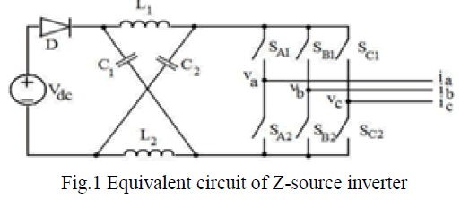 |
| It consists of two inductors and two capacitors to create impedance network, the function of inductors is to reduce current ripples and increase the non shoot through state voltage, the role of capacitor is to reduce the current ripples and to ensure a soft dc voltage at inverter input. Z-source inverter equivalent circuit as shown in figure1. |
| Impedance network acts like second order filter, is used to buck or boost input voltage and also improve the power factor, reduce harmonics, common mode voltage ,low inrush current. There is no additional equipment between source and load, so there is no additional loss. |
OPERATING PRINCIPLE OF Z-SOURCE INVERTER |
| It consists of two modes of operation |
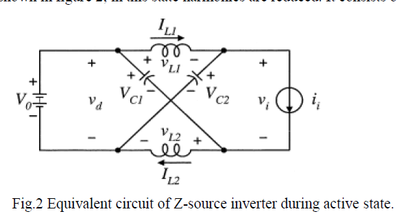
| Mode 1: During this mode of operation diode is conducting; energy is stored in inductors and capacitors. It is as active state in Z-source inverter shown in figure 2; in this state harmonics are reduced. It consists of six active states. |
 |
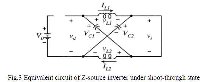
| Mode2: In this state diode is reverse biased, switches on in one phase leg then energy stored in inductors are boosted by energy stored in capacitor[1]. Here output voltage is higher than the input voltage. Fig.3 shows shoot -through state in Z-source inverter. It consists of one shoot-through state .In fig 3 represents two switches switched on in one phase leg. |
 |
CIRCUIT ANALYSIS |
 |
| The boost factor B is determined by the modulation index M .The boost factor B can be controlled by duty cycle of the shoot through zero state over the non shoot-through states of the PWM inverter. The shoot through state does not affect PWM control of the inverter. Because it equivalently produces the same zero voltage to the load terminal. The available shoot through period is limited by the zero state periods that are determined by the modulation index. |
| T= total switching interval, Vc=capacitor voltage, Output voltage can be stepped up and down by gain |
| Gain = M.B (11) |
BOOSTING TECHNIQUES |
| These are used to generate pulses for switching devices. Normally carried based PWM method is used in conventional inverter there is no voltage boost but in Z-source inverter shoot through state is introduced to get boost in output voltage by insert two constant values or envelopes [2]. The boosting techniques are (a) Simple boost Pulse Width Modulation method, (b) Maximum boost pulse width Modulation method and (c) Maximum Constant Boost pulse width modulation method. |
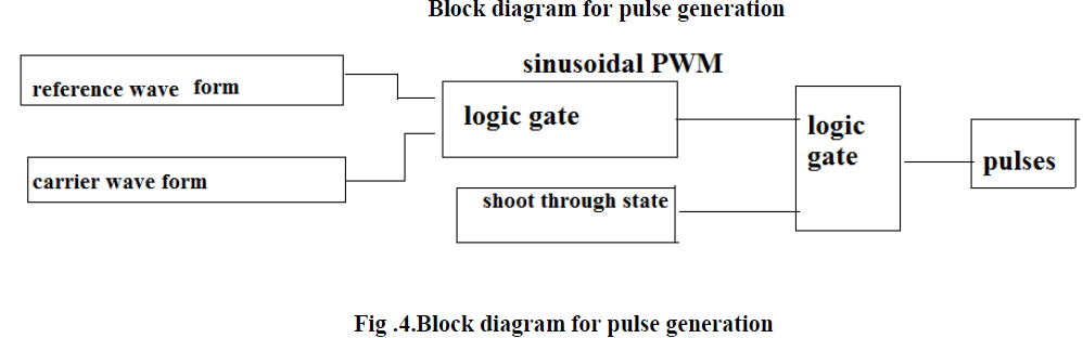 |
| In Fig .4 shows comparing reference wave form with carrier wave form (triangular wave form) we obtained sinusoidal pulse width modulation, this one is combined with shoot though state then we get pulses for switches which are used in main circuit. Shoot-through state is obtained when triangular wave compare with constant or envelope. |
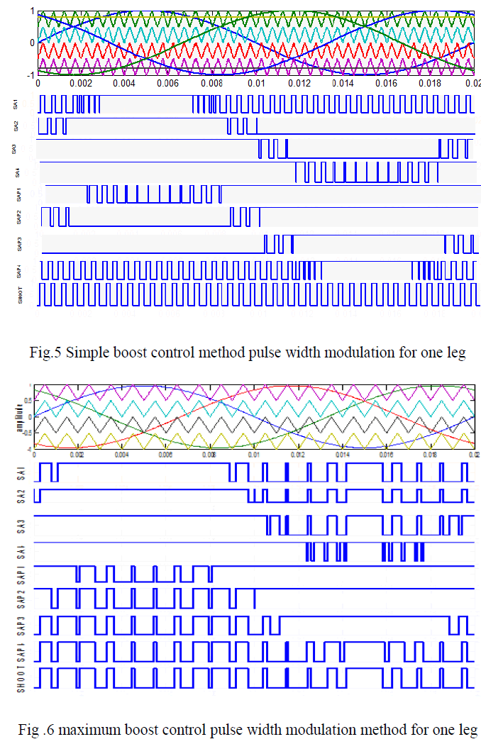
SIMPLE BOOST CONTROL METHOD |
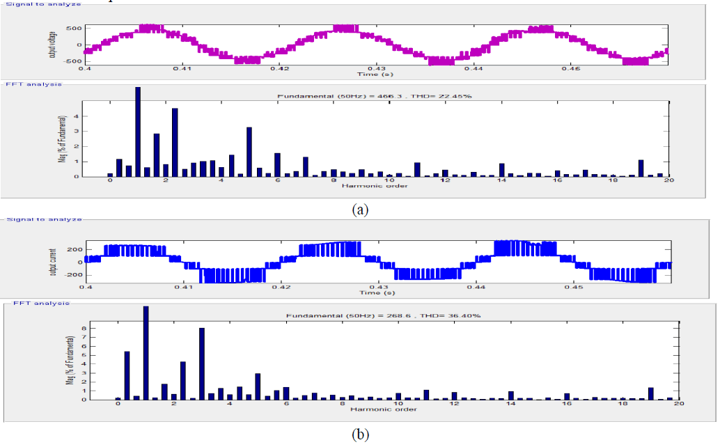
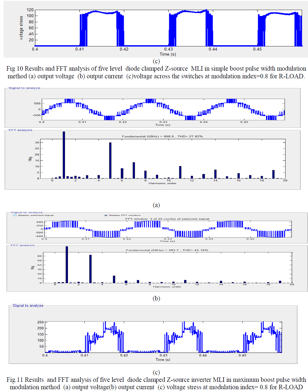
| It is a straight forward method, uncomplicated method. Figure 5 illustrates the simple boost control PWM. Here a straight line is equal to or greater than or lower than the peak values of reference wave forms to control the shoot through duty ratio[1][2]. All zero states are not utilized; duty ratio is limited to (1-M), M=modulation index. Whenever modulation index=1 no boost in voltage gain. Shoot –through state is inserting in sinusoidal PWM (as shown in fig 5) to obtained boost voltage. In simple boost produced output voltage with high gain, smaller modulation index, due to this obtained high voltage stress across switching devices as shown in fig 5. In this method voltage stress is high, it limits high voltage gain and also voltage rating of devices. These limitations are rectified by using maximum boost control method. |
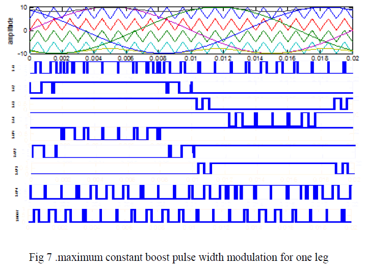
MAXIMUM BOOST CONTROL METHOD |
| In this method reducing voltage stress under a desired voltage gain becomes more important to control Z-source inverter [5]. All traditional zero states are converted to shoot through states, due to conversion minimize the voltage stress across the devices. This control method introduces low current ripples in inductor current and capacitor voltage, it gives high voltage gain and high modulation index as shown in fig 6. Maximum boost control method PWM, the shoot through interval state repeats periodically every 3 as shown in below fig 6. |
| In this method voltage stress across switching device is reduced at high modulation index, due to this, we get high voltage gain high boost factor [5].But inductor current and capacitor voltage consists of low frequency current ripples, due to this higher requirement of passive components THD, shoot through time interval are high to avoid disadvantages of this method, maximum constant boost control method is introduced. |
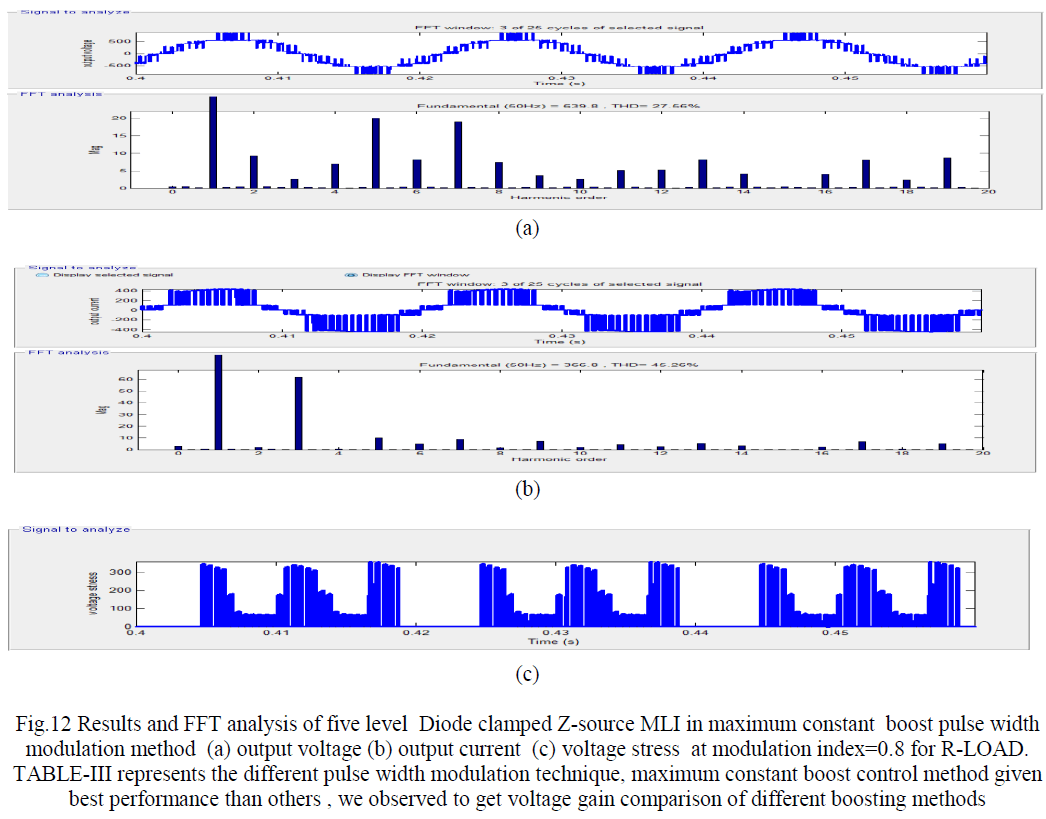
MAXIMUM CONSTANT BOOST CONTROL TECHNIQUE |
| This method consists of five modulating wave forms i.e. three reference waves (), two envelope wave forms .Shoot through state duty ratio is obtained when carrier triangular wave is greater than the upper envelope or lower than the lower envelopes shown in figure 7.By using this method to reduced the volume and cost of Z-source network, we need to eliminate the low frequency current ripples with constant duty ratio [7]. Here we get maximum boost factor at given modulation index and also voltage stress across the switches is reduced. |
| To get better results from constant boost control method than above two methods, and Modulation index and boost factor are increased and also high voltage gain voltage stress reduced not less than the maximum boost voltage. |
 |
 |
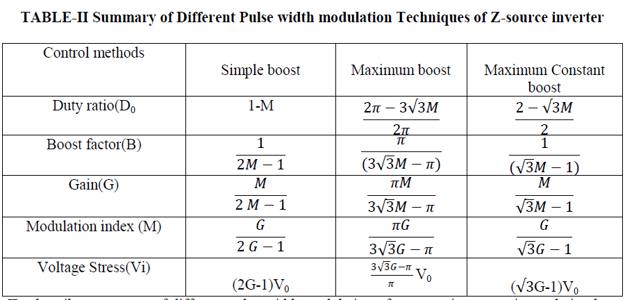 |
| In table –II describes summary of different pulse width modulation of z-source inverter, gives relation between duty ratio, gain, boost factor, voltage stress in terms of modulation index (M). |
MULTILEVEL INVERTER |
| In numerous applications requires high voltage gain, high power with reduced THD, voltage stress reduced with increment of levels. |
| Different topologies of multilevel inverter are |
| (1) Diode clamped multilevel inverter |
| (2)Flying capacitor multilevel inverter |
| (3)Cascaded multi level inverter. |
| In Z-source inverter during shoot through interval there is Voltage stress across the device is high, due to this voltage rating of device is increased. To reduce this problem Diode clamped multilevel inverter is used [11]. |
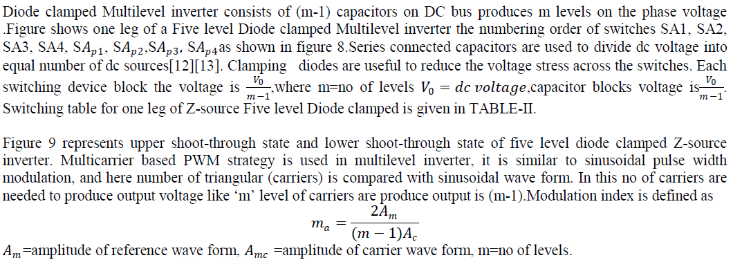
DIODE CLAMPED MULTILEVEL INVERTER |
 |
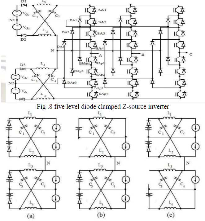 |
| Fig 9 (a) non shoot through state equivalent circuit (b) upper partial shoot through state equivalent circuit (c) Lower partial shoot through state equivalent circuit. |
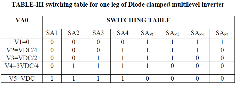 |
| Table –III describes switching devices operation in diode clamped multilevel inverter, upper switches (SA1,SA2,SA3,SA4) are turned off and lower devices (SAP1,SAP2,SAP3,SAP4)are turned on (0 means turned off,1 means turned on)then output voltage is zero. when lower devices are turnoff and upper devices are turn on output voltage is dc voltage VDC. |
SIMULATION RESULTS |
 |
 |
 |
 |
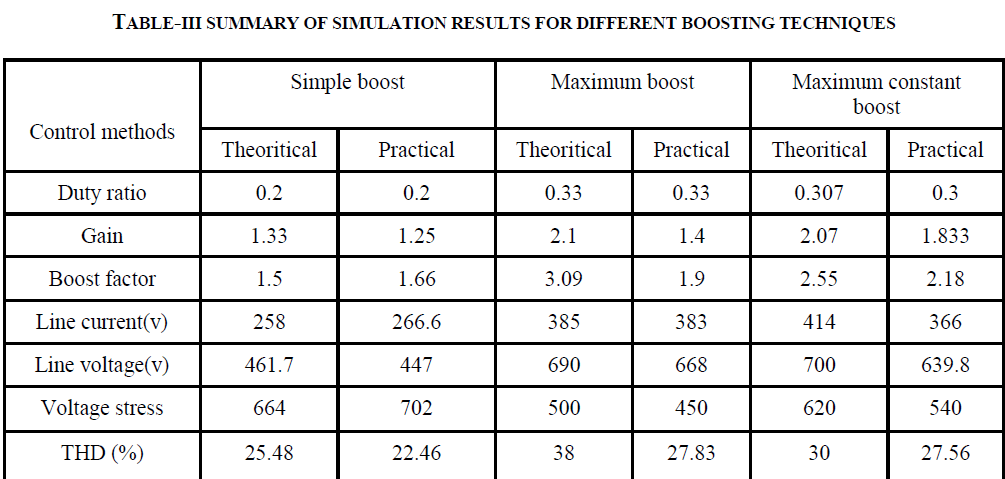 |
| Based on above analysis, the theoretical and practical values of different boosting techniques are listed in TABLE-III. In Table –III describes voltage stress reduced in maximum boost than compare to simple boost but there is one of the draw back i.e.it requires large size of passive components at low frequency so we go to maximum constant boost control method is used to reduced voltage stress and also harmonics reduced. |
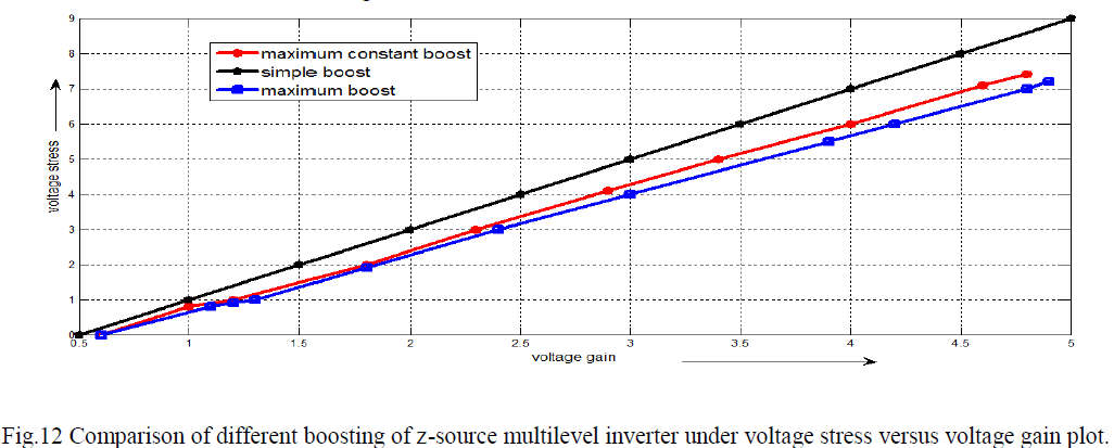 |
| From Figure12 in simple boost control method voltage gain increases automatically increased but at high modulation index there is no gain and also voltage stress across devices is high .To reduced voltage stress in maximum boost, but duty ratio is not constant, current ripple are occurred at low frequencies ,due to this complexity increases. These draw backs are rectified by using maximum constant boost control method and gives better performance than remaining two methods because voltage stress is reduced with high modulation index and high voltage gain . |
CONCLUSION |
| This paper presents five level diode clamped Z-source inverter. Three different pulse width modulation techniques are used to control of Z-source inverter to obtain high voltage gain, low THD and also reduced voltage stress across the devices three methods are simple boost, maximum boost & maximum constant boost control methods. Among them maximum constant boost control method gives better results than compare to remaining methods of pulse width modulation techniques, in terms of output voltage magnitude, THD and voltage stress across the device as no of levels increases with high voltage gain, low THD and reduced voltage stress. |
References |
|