International Journal of Advanced Research in Electrical, Electronics and Instrumentation Engineering
ISSN ONLINE(2278-8875) PRINT (2320-3765)
ISSN ONLINE(2278-8875) PRINT (2320-3765)
Divya S1, G.Umamaheswari2
|
| Related article at Pubmed, Scholar Google |
Visit for more related articles at International Journal of Advanced Research in Electrical, Electronics and Instrumentation Engineering
This paper deals with the voltage unbalance problem in multilevel inverters. Multilevel voltage source converters are the new trend in the power converter option for high-power applications. One of the major limitations of the multilevel converters is the voltage unbalance between different levels. The elimination of voltage unbalance in a single-phase five-level inverter which uses coupled inductors and feedback control, which can produce a five level output voltage with only one dc source. With this topology, splitting of the dc voltage is avoided, which eliminates the problem of voltage balancing in the circuit which was a prominent problem in the conventional topologies. The feedback control of the inverter is implemented using a PI controller. The six power switches used here have the same voltage stress and only one set of coupled inductors are adopted.
Keywords |
| Multilevel inverter, PI controller, Coupled inductor, Power switches, Voltage unbalance. |
INTRODUCTION |
| Multilevel converters are becoming an enabling technology in many industrial sectors. Multilevel converters have been under research and development for more than three decades and have found successful industrial application [1]-[5]. However, this is still a technology under development, and many new contributions and new commercial topologies have been reported in the last few years. One of the major limitations of the multilevel converters is the voltage unbalance between different levels. The techniques to balance the voltage between different levels in these types of inverters normally involve voltage clamping or capacitor charge control. These topologies use multiple dc voltage sources and multiple dc voltage capacitors [7], [8]. This is a great challenge when it comes to volume, weight, and cost minimization. The main problem with them is mainly the balancing of the dc capacitor voltages. The various applications of multilevel inverters: motor drives, active filters, power conditioning, energy storage in renewable energy systems, fuel cell energy systems, hybrid electric vehicles (HEV). |
| In all multilevel topologies with several DC link, the voltage balancing problem of DC capacitors was the key problem. The chopper circuit were used for DC capacitor voltage balancing in diode clamped multilevel inverters.[16] The most important are the topologies like diode clamped inverter, capacitor clamped, and cascaded multicell with separate DC source and the emerging topologies were asymmetric hybrid cells and soft switched multilevel inverters. The most relevant control and modulation methods developed for the family of converters are: multilevel sinusoidal pulse width modulation, multilevel selective harmonic elimination, and space vector modulation. [15] The most desirable topology is a multilevel inverter with only one dc source and no split capacitors but unfortunately this type of inverter has yet to be discovered .The voltage unbalance is a problem which reduces the efficiency of the output voltage in multilevel inverters [6],[9],[10]. The development of a multilevel inverter with better control unit will eliminate the problem of voltage unbalance. A single-phase five-level inverter using coupled inductors is studied in this paper. With the proposed inverter, only one dc voltage source is needed and split of the dc voltage capacitor is also avoided, which eliminates the problem of dc capacitor voltage balancing with the conventional topologies. Six power switches with the same voltage stress and only one set of coupled inductors are adopted [11]. It is, in fact, the adoption of the coupled inductors that makes it possible to generate an output of five-level voltage with only one dc voltage source. The presented topology is very suitable for low to medium power applications and also for high-current cases. In an open loop system the errors in the output are not rectified automatically. The use of a closed loop system helps to attain a better quality output with improved control features. A pi controller unit is chosen in order to realize the closed loop configuration [13]. The voltage and current outputs from the proposed inverter are fed back to the controller. The pi controller processes its available data, compares it with the preset reference value and calculates the deviation from the ideal working condition [14],[15]. The rectification is made by the controller by the switching pattern control and firing control of the switching elements used in the inverter topology. Thus an improved output waveform with reduced distortion and better controllability with reduced number of switches and with no voltage unbalance problem is obtained. |
SINGLE PHASE MULTILEVEL INVERTER WITH COUPLED INDUCTORS AND FEEDBACK CONTROL |
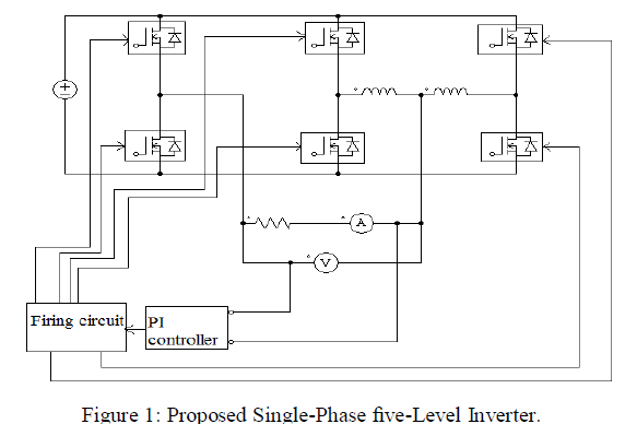 |
| The figure 1 represents the circuit diagram of the inverter using coupled inductors. 2E is the dc input voltage and L; and L& are the two coupled inductors. The mutual inductance of the two inductors is M and the output terminals of this inverter are 1 and 2. Obviously, this topology is very simple and can be constructed simply by the addition of a coupled inductor to a conventional three-arm inverter bridge. It is the adoption of the coupled inductors that makes it possible to output five-level voltage with only one dc voltage source. Suppose that the two coupled inductors are with the same number of turns or obtained by a center-tapped inductor. |
| The leakage inductances of the two inductors are Lσ1 and Lσ2, respectively. Assuming that Lσ; = Lσ =Lσ , the voltage equations of the coupled inductors can be expressed as follows: |
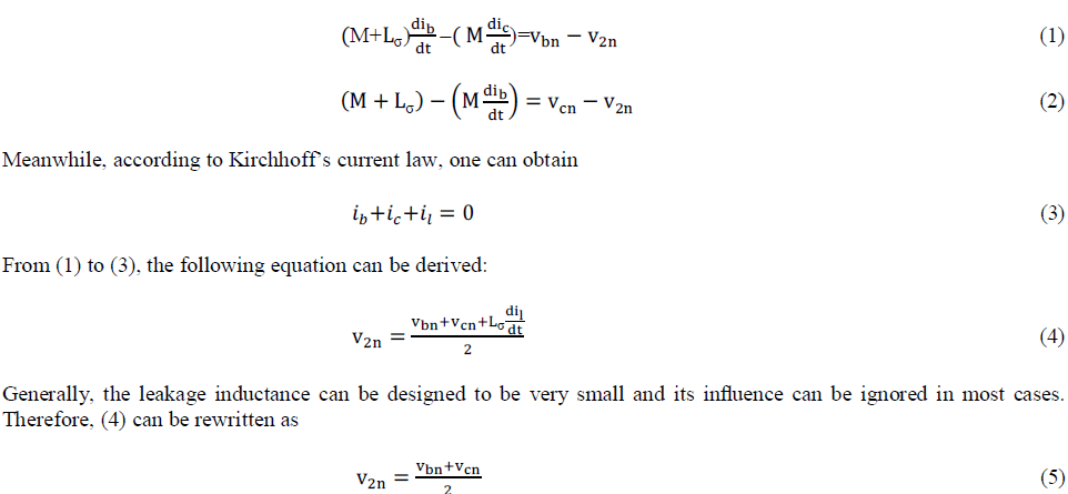 |
| This result is interesting and shows that the coupled inductors will perform as an adder of the two input voltage at the non-common-connected terminals with the common-connected terminal as the output. Actually, without the help of the coupled inductors, the proposed inverter will not be able to output five-level voltage. The power switches in one arm are assumed to switch complementarily. For instance, Smust be turned OFF if S is turned ON and vice versa. |
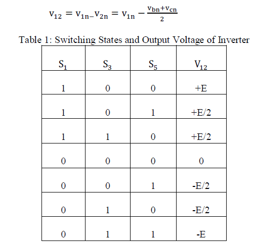
| So the following discussion will only focus on the switching states of the switches S, S, and S. For convenience of analysis, the number “1” will be used to denote the ON state of one switch and “0” will be used to denote the OFF state. In fact V1n, Vbn, and Vcn all can generate two-level voltage (+E and −E). According to (6), the voltage levels of V12 can be summarized in Table 3.1. The proposed inverter can generate five voltage levels at its output terminals. From Table 3.1, it should be pointed out that the switching state of S must be 1 if V12 ≥ 0 and the switching state of S must be 0 if V12 ≤ 0. This means Sand S will switch at the fundamental frequency of the reference signal. So, the switching losses of S and S will be very low in the proposed inverter. The output voltage of the proposed inverter can be expressed as |
 |
DESIGN OF THE COUPLED INDUCTORS |
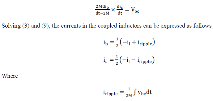
| In order to design the coupled inductors, the relationship between the currents of the coupled inductors i, iand the load current i should be analyzed. Using (1) and (2) and neglecting the leakage inductance, one can obtain |
 |
 |
FEEDBACK CONTROL |
| The first arm of the circuit is given gating signals using pulse generator. The next two arms which have the coupled inductor is the main part of the circuit. Actually, without the help of the coupled inductors, the proposed inverter will not be able to output five-level voltage. So the feedback control is provided only to the last two arms. The output voltage and current are used to realize the closed loop control. This is done using the pi controller and comparator unit. Thus by implementing a closed loop control, the output voltage quality is improved and it remains steady for any type of load condition. Since there is no use of dc link capacitors in this circuit, the problem of voltage unbalance is eliminated. The gating signals are given to the MOSFETS in the second and third arm by comparing the output voltage wave with a triangular wave. From the fourier analysis of the circuit it can be shown that the THD decreases. The voltage unbalance in the circuit is eliminated. |
| The proposed single-phase five-level inverter is based on coupled inductors. This inverter can output five-level voltage with only one dc source and no split of the dc voltage capacitor, totally avoiding the voltage balancing problem. The height of the staircase in the output voltage is only half of the dc-link voltage under any modulation index. Meanwhile, the voltage stresses on all the power switches are the same and only four switches are operated at high frequency. It is, in fact, the adoption of the coupled inductors that make it possible to output five-level voltage with only one dc voltage source. No split of the dc voltage capacitor is needed, totally avoiding the voltage balancing problem in conventional multilevel inverters. Six power switches with the same voltage stress and only one set of coupled inductors are adopted. This inverter is based on the widely used three-arm power module and the voltage stresses on all the power switches are the same, making it very easy to construct. The presented topology is very suitable for low to medium power applications, especially for high-current cases. |
RESULT AND DISCUSSION |
 |
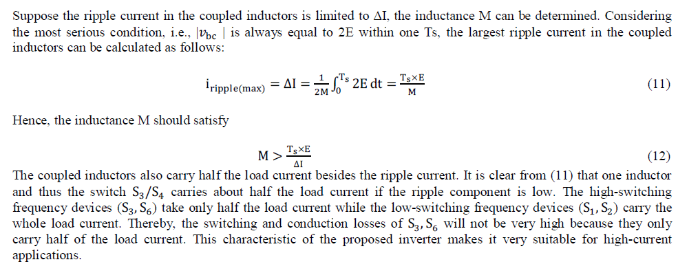
| The output of the multilevel inverter presented here is a five level voltage. The output voltage is taken across the loadconnected across the common and non common terminal. The absence of voltage unbalance in the output voltage is visible from the output voltage waveform. The presence of coupled inductor is the main element responsible for the generation of five level output voltage using just six switches. This output voltage is taken as the feedback signal to the PI controller. The output waveform for 100V DC input is given above. A five stage output is obtained. The voltage levels are 100V, 50V, 0V, -50V, -100V. These levels are shown in the graph above. |
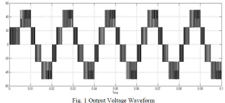
| The current through the load arm is measured. The output current waveform is obtained by connecting a current source in series with the load. The current is in the range of milli amperes. The value of the current is 0.025mA. The current ripples are absent and it is clear from the output waveform. This current waveform is also fed to the PI controller as feedback signal. The PI controller unit processes the voltage and current waveforms to generate the firing pulses. |
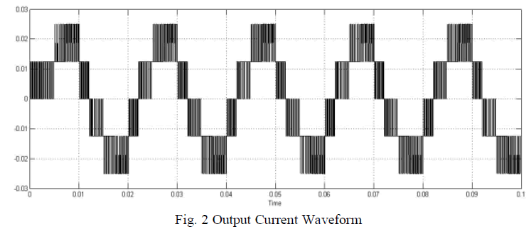 |
| The firing pulses as given to the MOSFETS in the order of s1, s2, s3, s4, s5 and s6 are given in the graph shown above. The firing pulses for the first arm are given using pulse generators and the firing pulses to the other arms are given using feedback. |
 |
| The firing pulses are generated by comparing the output of the PI controller with the triangular wave. This process is done inside the subsystem. The switches in the first arm are provided with the firing pulses using pulse generators. The switches in the other two arms are given firing pulse by the comparison of the output of the PI controller with a triangular wave; this process is done inside the subsystem. |
CONCLUSION |
| The proposed single-phase five-level inverter is based on coupled inductors and closed loop configuration. This inverter can output five-level voltage with only one dc source and no split of the dc voltage capacitor, totally avoiding the voltage balancing problem. The FFT analysis of the proposed circuit in the closed loop conditions shows the THD values of the system. |
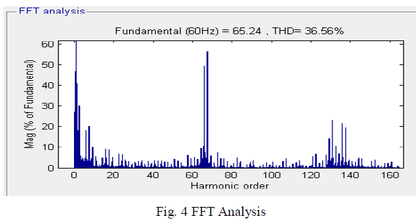 |
| The closed loop control in the proposed system uses both the voltage and current feedback. From the FFT analysis the THD value of the circuit has been obtained as 36.56 % and hence it is proven that the proposed system is more efficient. Verification of the results show validity of the proposed topology and the feedback control. |
References |
|