International Journal of Advanced Research in Electrical, Electronics and Instrumentation Engineering
ISSN ONLINE(2278-8875) PRINT (2320-3765)
ISSN ONLINE(2278-8875) PRINT (2320-3765)
Manju Mohan1, Bini D2
|
| Related article at Pubmed, Scholar Google |
Visit for more related articles at International Journal of Advanced Research in Electrical, Electronics and Instrumentation Engineering
This design describes a wide range voltage to frequency converter in a single PSoC chip, which can measure wide range of voltage between 50mV-5000mV and found suitability in sensor applications. This design is implemented in a PSoC3 device IC CY8C3866. The design implements analog and digital user modules: an IDAC, COMPARATOR, PWM, COUNTER, UART and LCD. The comparator gets the analog input from measurement signal or from sensors and the digitized output is sent to serial port through UART module. User friendly menu driven program written in LABVIEW acquires the serial data from PSoC chip and the acquired measurement data is displayed on the PC menu screen as well as saved in a user specified file path. The user interacts only with the graphical screen designed for the project. The software used is PSoC creator 2.2 and LabVIEW.
Keywords |
| LABVIEW, PSoC, Transfer Characteristics, Virtual Instrument, V to F Converter. |
INTRODUCTION |
| A Voltage to Frequency Converter is a device which can accept an analog voltage or current signal as input and converts it into an equivalent digital signal. The frequency of the digital signal is linearly proportional to the measured input voltage or current signal. It is advantageous to transmit a digital signal rather than an analog signal for long distance communications due to high noise immunity. This paper describes a wide range voltage to frequency converter design implementation in a single Programmable System on Chip (PSoC), which can measure wide range of voltage between 50-5000mV and found suitability in sensor applications. This design is implemented in a PSoC3 device IC CY8C3866. The unique design feature in PSoC design is the implementation of analog and digital user modules in a single chip, example in this design are: an IDAC, COMPARATOR, PWM, COUNTER, UART and LCD modules implemented within PSoC chip. The comparator gets the analog input from measurement signal or from sensors and the digitized output, converted using IDAC, PWM and COUNTER modules, and is sent to serial port through UART module. User friendly menu driven program written in LABVIEW acquires the serial data from PSoC chip and the acquired measurement data is displayed on the PC menu screen as well as saved in a user specified file path. The user interacts only with the graphical screen designed for the project. The software design toll used for the programmable hardware is PSoC creator 2.2. |
RELATED WORK |
| Voltage-to-frequency (V/F) is widely used in applications such as industrial electronics, frequency-shift keying modulators, Phase-locked systems, analog-to digital converters, and isolation amplifiers. Voltage-To-Frequency Converters are low cost circuits for analog-to-digital conversion that generates a pulse train at a frequency precisely proportional to applied input voltage. |
| Standalone ICs are used in the existing systems. TC9400/9401/9402 is a low cost V to F converter which accepts analog voltage as input and generates a train of pulses whose frequency is proportional to the input voltage. Even though these converters are produced as standalone devices, they still require several external components and are relatively expensive compared to modern low-cost analog integrated circuits. At present as an intelligent system design PIC, 8051 or in general any microcontroller is usually applied for voltage to frequency converter, but it requires many external components for the application. In this paper, PSoC3 microcontroller is used for wider V to F conversion which allows the designer to build the V/F converter using a PSoC microcontroller with its internal user modules and an external capacitor for charging. The PSoC Creator tool is given a useful device function with virtually no additional cost or extra components. |
PROGRAMMABLE SYSTEM ON CHIP |
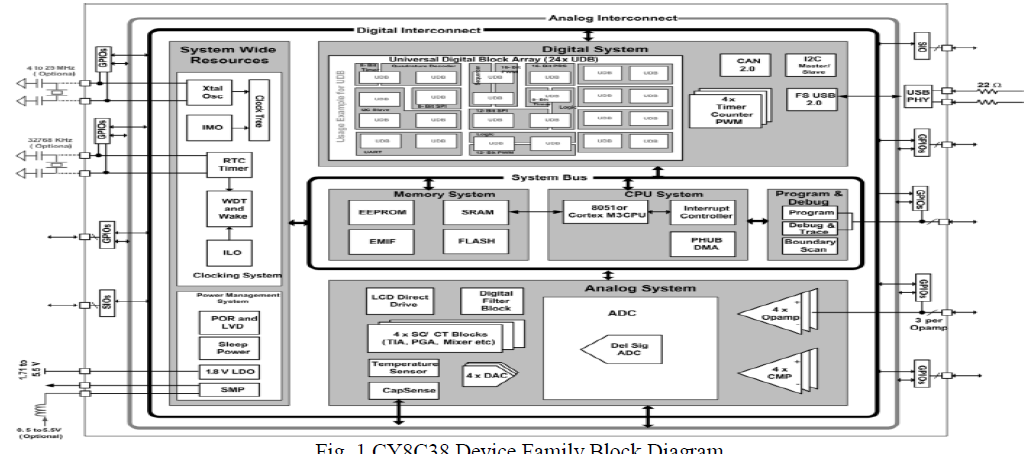
| A Programmable System on Chip (PSoC) is software configured, mixed-signal array with a built-in MCU core. PSoC facilitates an advanced method of signal acquisition, processing and control with exceptional accuracy, high bandwidth and superior flexibility. Its analog capability spans the range from thermocouples (DC voltages) to ultrasonic signals. The digital, analog and mixed signal blocks are all built on the same chip. In fig 1, CY8C38 device family block diagram is shown. PSOC 3 (CY8C38xxxx, CY8C36xxx, CY8C34xxx, CY8C32xxx) families are fully scalable 8-bit PSoC platform devices that have these characteristics: An 8-bit single cycle pipelined 8051 processor, running up to 67 MHz, with a nested vectored interrupt controller(NVIC) and a high-performance DMA controller. The single cycle 8051 CPU runs ten times faster than a standard 8051 processor. Digital system includes configurable Universal Digital Blocks (UDBs) and specific function peripherals, such as USB, CAN and I2C. PSoC has three separate memory spaces: paged SRAM for data, Flash memory for instructions and fixed data and I/o Registers for controlling and accessing the configurable logic blocks and functions. The device is created using SONOS technology. |
A. PSoC Designer |
| PSOC designer is the first generation software IDE to design, debug and program the PSoC 1 devices. It introduces unique features including a library of pre-characterized analog and digital peripherals in a drag-and-drop design environment which could then be customized to specific design needs by leveraging dynamically generated API libraries of code. |
B. PSoC Creator |
| PSoC Creator is the second generation IDE to design debug and program the PSoC 3 and PSoC 5 devices. The development IDE is combined with an easy to use graphical design editor to form a powerful hardware/software codesign environment. PSoC Creator consists of two basic building blocks. The program that allows the user to select, configure and connect existing circuits on the chip and the components which are the equivalent of peripherals on MCUs. The configurable blocks in a PSoC are the biggest difference from other microcontrollers. PSoC devices include up to 16 digital and 12 analog blocks, depending on the device. Fig. |
 |
DESIGNING IN PSoC CREATOR |
| To create a new project, click “Create New Project” on the Start Page. On the New Project dialog, select an empty design and complete the requested project information. We can select a Starter Design to create a new project with components and code already placed. Components are to be selected and dragged from the Component Catalogue onto the schematic design. Various component parameters are configured to modify the behaviour as needed. A Pins component, Clock component and other components are added to complete the design. Various components are connected using the Wire tool. Once completed, use the Build command to generate source code. Components used in the design of Voltage-Frequency Converter are: |
| IDAC |
| Comparator |
| PWM |
| Counter |
| UART |
| LCD Display |
| Features of IDAC: The IDAC8 component is an 8-bit current output DAC (Digital to Analog Converter). The output can source or sink current in three ranges. The IDAC8 can be controlled by hardware, software or by a combination of both hardware and software. |
| Three ranges: 2040 ìA, 255 ìA and 31.875 ìA |
| Current sink or source selectable |
| Software- or clock-driven output strobe |
| Data source may be CPU, DMA or Digital components |
| Features of Comparator: The comparator (comp) component provides a hardware solution to compare two analog input voltages. The output can be sampled in software or digitally routed to another component. Three speed levels are provided to allow optimizing for speed or power consumption. A reference or external voltage can be connected to either input. We can also invert the output of the comparator using the Polarity parameter. |
| User controlled offset calibration |
| Multiple speed modes |
| Low-power mode |
| Output routable to digital logic blocks or pins |
| Selectable output polarity |
| Configurable operation mode during Sleep |
| Features of PWM: The PWM component provides compare outputs to generate single or continuous timing and control signals in hardware. The PWM provides an easy method of generating complex real-time events accurately with minimal CPU intervention. PWM features may be combined with other analog and digital components to create custom peripherals. |
| 8-bit or 16-bit resolution |
| Multiple pulse width output modes |
| Configurable trigger |
| Configurable capture |
| Configurable hardware/software enable |
| Features of Counter: The Counter component provides a method to count events. It can implement a basic counter function and offers advanced features such as capture, compare output and count direction control. For PSoC 3 and PSoC 5 devices component can be implemented using FF blocks or UDB. PSoC 4 devices support only UDB implementation. A UDB implementation typically has more features than an FF implementation. If the design is simple, consider using FF to conserve UDB resources for other purposes. |
| Fixed-Function (FF) implementation for PSoC 3 and PSoC 5 devices |
| 8-, 16-, 24-, or 32-bit counter |
| Up, down or up-down configurations |
| Optional compare output and capture input |
| Enable and reset inputs for synchronizing with other components |
| Features of UART: The UART provides asynchronous communications commonly referred to as RS232 or RS485. The UART component can be configured for Full Duplex, Half Duplex, RX only or TX only versions. All versions provide the same basic functionality. They differ only in the amount of resources used. To assist with processing of the UART receive and transmit data, independent size configurable buffers are provided. |
| 9-bit address mode with hardware address detection |
| Baud rates from 110 to 921600 bps or arbitrary up to 4 Mbps |
| RX and TX buffers = 4 to 65535 |
| Detection of Framing, Parity and Overrun errors |
| Full duplex, Half Duplex, TX only and RX only optimized hardware |
| Features of LCD: The Character LCD component contains a set of library routines that enable simple use of one, two or four-line LCD modules that follow the Hitachi 44780 standard 4-bit interface. The component provides APIs to implement horizontal and vertical bar graphs. |
| Implements the industry-standard Hitachi HD44780 LCD display driver chip protocol |
| Requires only seven I/O pins on one I/O port |
| Contains built-in character editor to create user-defined custom characters |
LABVIEW |
| Laboratory Virtual Instrumentation Engineering Workbench is a platform and development environment for a visual programming language from National Instruments. The graphical language is named “G” Language which is a unique tool implementing the data-flow programming model. In this project, LabVIEW has been used for giving a graphical user interface and also for communicating with PSoC through the Serial Port of the computer. LabVIEW provides a set of functions in the Function palette which is used for establishing a Serial Communication buffer and closing the Serial Communication operation. With LabVIEW, visualizing the program flow becomes easier and hence leads to faster and more efficient coding. LabVIEW provides excellent debugging tools and huge support through official forums. LabVIEW programs are called virtual instruments (VIs). Vis contains three main components-the Front panel, the block diagram and the Icon & Connector pane. The front panel is the user interface of the VI. The controls and functions contain sub palettes of objects to create a VI. |
EXPERIMENTAL SETUP |
| The basis for voltage-to-frequency converter uses the principle of linear charging and discharging of capacitance. The circuit consists of a charging capacitor, programmable current source, a comparator, PWM and counter. |
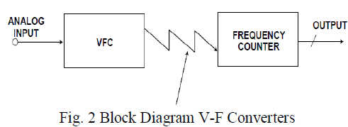 |
| The current set by IDAC module charges the external capacitor linearly until the threshold voltage is reached. The output frequency is dependent on capacitance value and the changing current. For the measurement, a Pulse Width Modulator (PWM) of a fixed period is enabling a 16-bit counter. The output of comparator clocks the counter and the count value is read and sent to Universal Asynchronous Receive transmit (UART) for transmitting to PC. |
PSoC IMPLEMENTATION FOR V TO F CONVERTER |
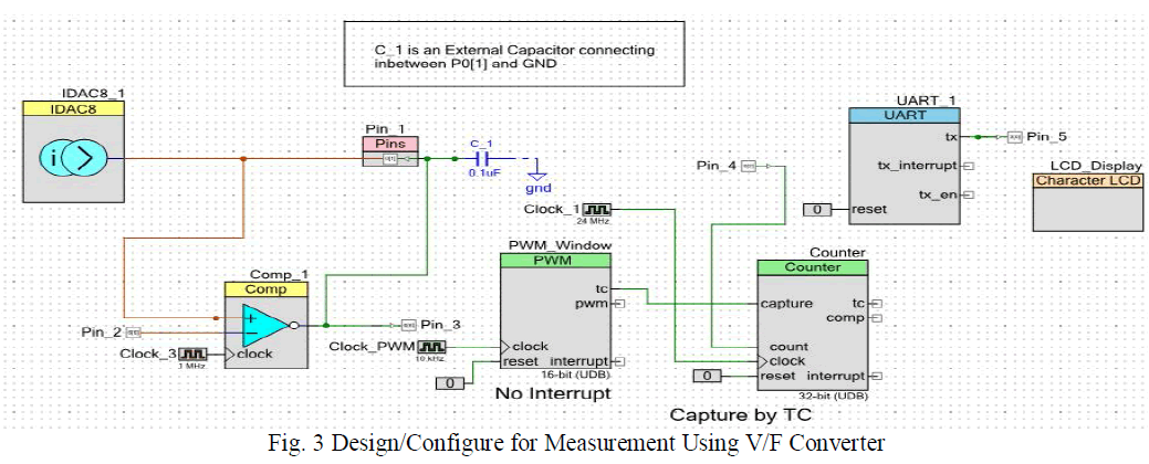
| In fig 3, the implementation of wide range voltage to frequency converter using PSoC3 microcontroller is shown. In this method, input voltage from the programmable voltage source is given to the input of the comparator. When output of comparator is High, IDAC output is connected to the pin. When comparator output is low, the pin shorts to ground. IDAC has been configured as a current source. IDAC charges the external capacitor connected to C_1. When the capacitor voltage crosses input voltage Vin, comparator output becomes low an discharges the capacitor. As capacitor voltage becomes zero, the comparator output becomes high and IDAC starts charging the capacitor. The cycle continues and we get an oscillator whose frequency is inversely proportional to Vin. The period of the output waveform is directly proportional to the input voltage. The frequency output of the circuit can be found from the formula: |
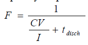 |
| where, F is the output frequency, C is the capacitance, V is the input voltage, I is the IDAC current and tdisch is the period of the Comparator’s Synch clock. The frequency measurement is the number of rising edges that occur within one second. The project uses a PWM to generate the time window. The signal whose frequency is to be found is given to the count input of the counter. The count value in the counter within the time window gives a measure of the input signal frequency. The calculated frequency is displayed on the LCD Display and the UART provides asynchronous communications to PC via RS 232. |
 |
LABVIEW IMPLEMENTATION FOR VOLTAGE TO FREQUENCY CONVERTER |
| In this design, LabVIEW has been used for giving a graphical user interface and also for communicating with PSoC through the serial port of the computer. The measured data is displayed in the menu screen as well as saved in a user specified file path. |
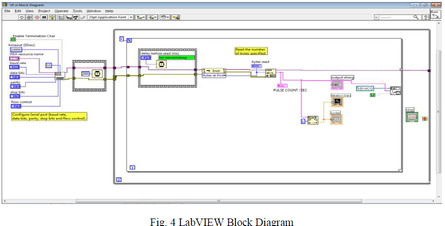 |
| Fig 4 shows the block diagram in LabVIEW. The block diagram mainly consists of a VISA Configure serial port (initializes the serial port to the required settings given), VISA Read (Reads the specified number of bytes from the device or interface specified by VISA resource name and returns the data in read buffer) and a waveform chart(generates a waveform with voltage along X-axis and counts along Y-axis). |
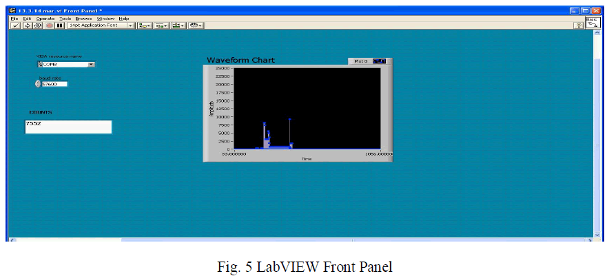 |
| Fig 5 shows the front panel in LabVIEW. The user enters the inputs through the interface or front panel which is also the screen on which the outputs are displayed. |
RESULTS |
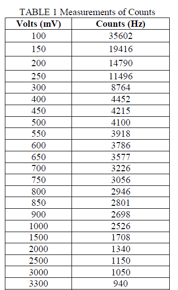
| Voltage to Frequency converters generates a digital output proportional to the measured input voltage or current signal. Table 1 shows the measurements of counts corresponding to the input voltage given. |
 |
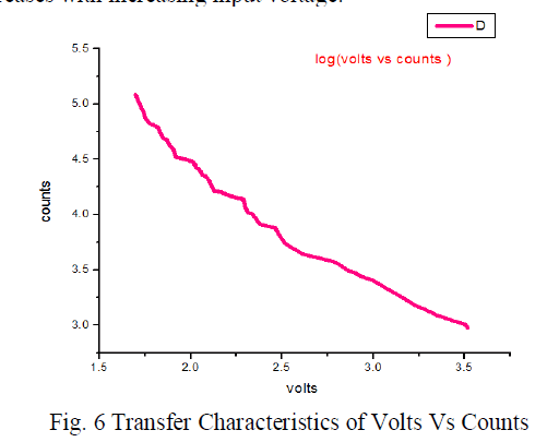
| Fig 6 shows the transfer characteristic as a function of the input voltage. The frequency has been measured for various input voltages. The slope decreases with increasing input voltage. |
 |
CONCLUSION |
| A wide range Voltage to Frequency Converter has been designed and implemented using the PSoC components and configurations. The results are quite accurate and the device is operable in any operating environment. The main advantage of this design over others is that it uses just one chip for the entire operation. The repeatability during tests has been verified. There is a scope for developing the design to be able to measure the voltages in the range of nano volts. |
References |
|